


An integrated bifunctional metamaterial perfect absorber for high-efficient broadband absorption and narrowband refractive index detection
 0
0 Abstract
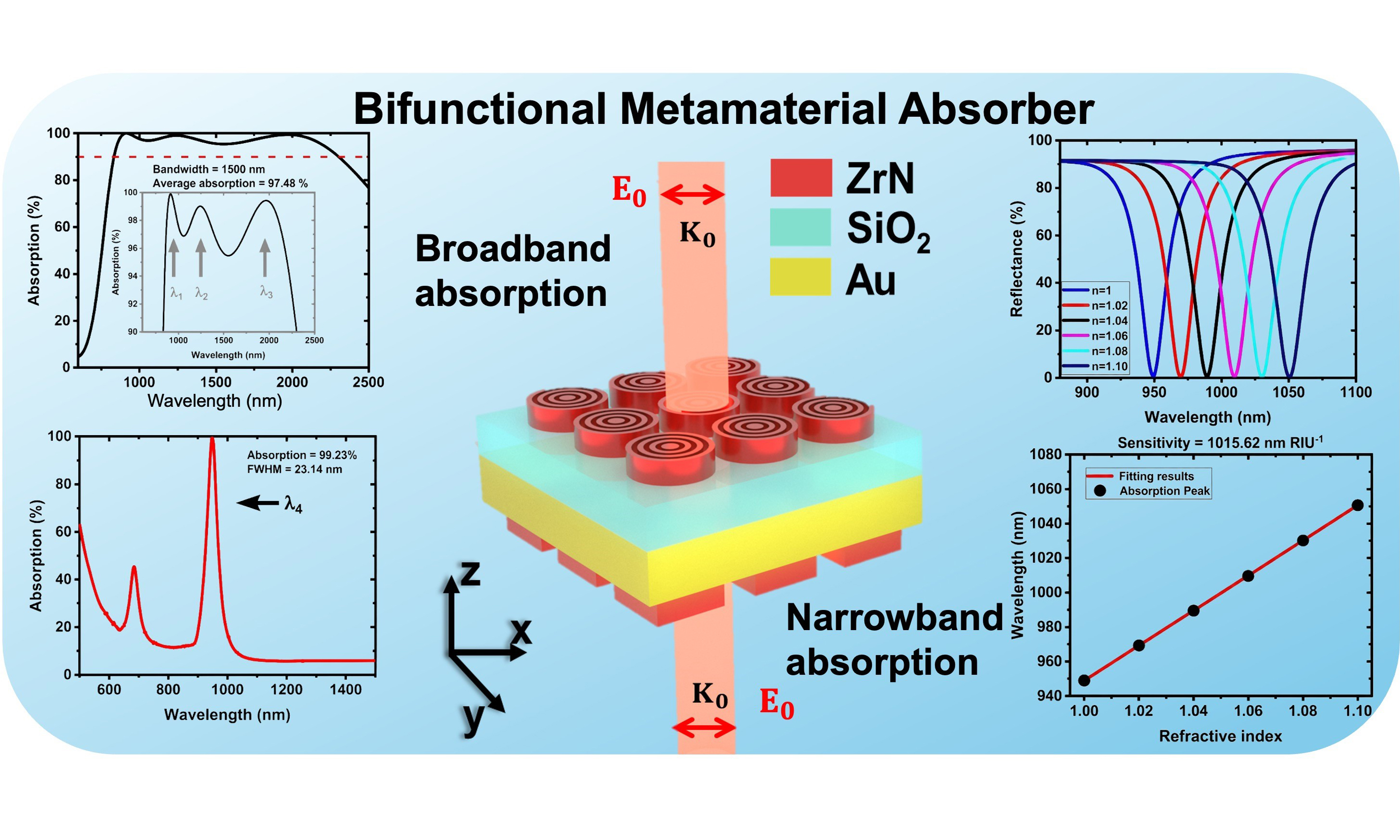
Metamaterial absorbers have been extensively investigated for broadband light harvesting and narrowband sensing, but integrating both into one compact device still remains challenging. In this work, we propose a bifunctional metamaterial absorber (BMA) based on zirconium nitride (ZrN). The device consists of periodically arranged ZrN concentric-ring arrays on a silicon dioxide (SiO2) spacer with an Au film underneath for broadband absorption, and ZrN-based four-by-four square-grid arrays on the opposite side of the Au substrate for narrowband refractive index sensing. Numerical simulations show that the broadband mode achieves an average absorptivity of 97.48% over the wavelength range of 800 to 2,300 nm, while the narrowband mode exhibits a near-perfect absorptivity at 948.1 nm with a bandwidth of 23.14 nm, delivering a sensitivity of 1,015.62 nm RIU-1. Electric field distributions and impedance analyses indicate that the absorption behavior arises from the couplings of localized surface plasmon resonances, multipole resonances, and Rayleigh Anomalies (RAs). Parametric studies demonstrate that the broadband absorption maintains high absorptivity in a wide wavelength range, whereas the narrowband resonance systematically shifts as the varying structural parameters. These results not only highlight the importance of integrating light harvesting and refractive index sensing in a single design, but also pave the way for incorporating multiple functionalities into one compact device for broad applications.
Keywords
INTRODUCTION
Metamaterials, artificially engineered periodic structures that are unattainable in natural materials, exhibit distinct electromagnetic[1,2], acoustic[3,4], and mechanical responses[5,6]. Since the first report by Landy et al.[7] in 2008, metamaterial absorbers have attracted considerable attention due to their ability of achieving near-perfect absorption of electromagnetic radiation through precisely engineered subwavelength structures[8-11]. Recently, inverse design has significantly boosted the development of perfect metamaterial absorbers by enabling non-intuitive geometries and hybrid absorption mechanisms[12,13]. Owing to their narrowband and broadband absorption capabilities, metamaterial absorbers enable diverse applications. Specifically, broadband metamaterial absorbers have been widely adopted for solar energy harvesting, thermophotovoltaic conversion, and electromagnetic interference suppression[14-17]. By contrast, narrowband metamaterial absorbers demonstrate obvious advantages in refractive index sensing, biomedical detection, and environmental protection[18-21]. For instance, Wu et al. reported an efficient broadband solar absorber based on a checkerboard-shaped TiN grating embedded in SiO2. It achieves an average absorptivity of 97% from 0.4 to 2.0 μm[15]. Kang et al. proposed an ultra-narrowband metamaterial perfect absorber consisting of an array of Au cross-type nanostructures separated from a continuous Au ground layer by a SiO2 spacer. Its peak absorption is tunable in the infrared spectral region while maintaining at a high absorptivity of 99.7%[22]. However, these metamaterial absorbers generally offer a sole function, which limits their utilization in practical applications. A compact device integrating both broadband and narrowband absorption within a single platform has seldom been reported. Gao et al. demonstrated a bifunctional absorber that combines nanopatterned gold arrays on the top side with a four-layer metal-dielectric-metal-dielectric configuration on the bottom side[23]. In this device, the figure of merit (FOM) for refractive index sensing is only 37 RIU-1. Meanwhile, the broadband mode exhibits an absorptivity of 84.09% over a relatively narrow bandwidth (400 to 900 nm). However, current bifunctional absorbers still suffer from critical limitations. First, they develop on noble metal platforms with limited thermal robustness. Second, they fail to strike an adequate balance between broadband absorption and narrowband sensing performance. Third, they lack differentiated designs that allow these two functionalities to be optimized separately within one compact device. Most of the conventional metamaterial absorbers employ noble metals such as gold and silver. The inherent drawbacks of noble metals have spurred the search for plasmonic materials with superior thermal and chemical stability[24,25]. In recent years, transition metal nitrides have attracted significant attention due to their favorable optical properties, thermal stability, chemical inertness, and mechanical robustness[26,27]. Among them, ZrN exhibits metallic properties with low electrical resistivity[28,29] and higher thermal stability than noble metals[30]. Despite these merits, ZrN-based metamaterials have seldom been investigated, and their potential for simultaneous broadband absorption and narrowband refractive index sensing remain unexplored.
In this work, we propose a BMA constructed from plasmonic ZrN. The BMA adopts a double-side architecture: A concentric-ring array is patterned on one surface of an Au/SiO2 supported substrate for broadband absorption, while a four-by-four square-grid array is fabricated on the reverse surface for narrowband refractive index sensing. Distinct from previously reported bifunctional absorbers, our design adopts a structurally differentiated, double-sided architecture constructed from transition-metal-nitride material. This configuration enables the broadband and narrowband functions to be independently excited and optimized within one compact device. The proposed BMA delivers an average broadband absorptivity of 97.48% over the wavelength range from 800 to 2,300 nm. In its narrowband mode, the device achieves a near-perfect absorption peak of 99.23% at 948.1 nm and a refractive index sensitivity of 1,015.62 nm RIU-1. Electromagnetic field distributions at the resonant wavelengths and impedance matching are systematically analyzed to elucidate the underlying physical mechanisms. This work not only presents a high-performance bifunctional absorber, but also provides profound physical insights for developing advance the integration of light harvesting and precision sensing within a compact metamaterial platform.
MATERIALS AND METHODS
Figure 1A and B display the schematics of the proposed BMA. The device consists of a SiO2 spacer layer and an Au isolation layer, with ZrN meta-atom arrays arranged on both surfaces. Under normally incident illumination, the top surface provides broadband absorption while the bottom surface provides narrowband absorption. The broadband meta-atom consists of periodically arranged concentric rings. The radii of these three concentric rings are denoted as R1, R2, and R3, with a constant ring width (r) and the same thickness (h) in Figure 1C. The narrowband meta-atom consists of a regular four-by-four square-grid array, as shown in Figure 1D. The length and the side width of each square grid are labeled as L and W, respectively. By adjusting these parameters, both broadband and narrowband perfect absorption peaks can be achieved within the same wavelength range. The absorptivity (A) of the BMA is calculated from the reflectivity (R) and transmissivity (T) according to A = 1 - R - T. Perfect absorption is achieved when both reflectance and transmittance are negligibly small or approach zero. In the proposed design, the reflectance is suppressed by impedance matching while the transmittance is blocked by the underlying metal layer.
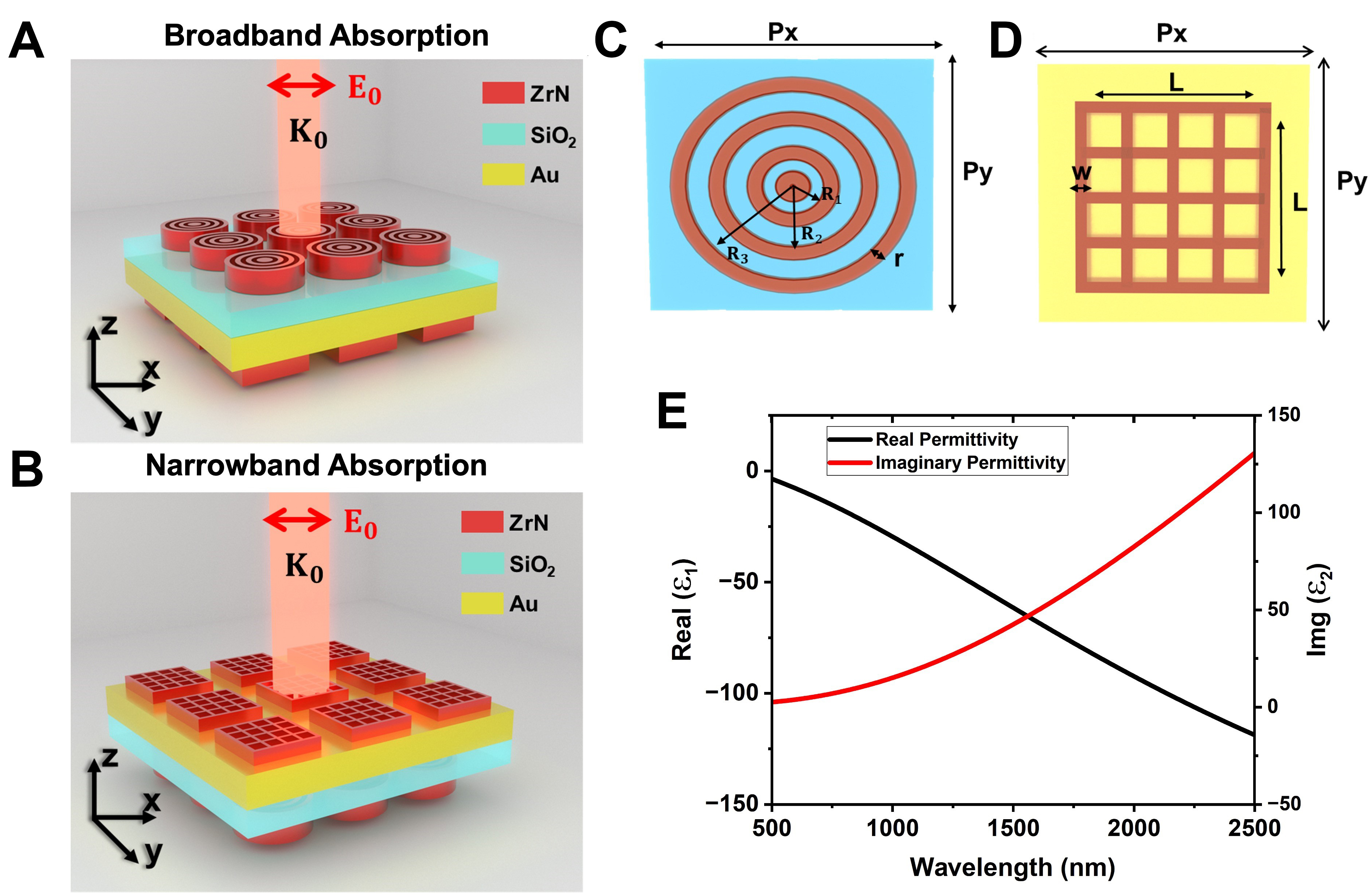
Figure 1. Schematic diagram of the BMA’s broadband metamaterial absorber (A) and narrowband metamaterial absorber (B) based on ZrN under vertical incidence, the schematic of the meta-atom for broadband (C) and narrowband (D) absorption. Real and imaginary parts of the relative permittivity (E) of ZrN. BMA: Bifunctional metamaterial absorber; ZrN: zirconium nitride.
The absorption properties of the near-infrared BMA were investigated using the three-dimensional finite-difference time-domain (FDTD) method. Simulation modeled the interaction between incident light and the ZrN metamaterial over the wavelength range of 500 to 2,500 nm. Periodic boundary conditions were applied in the x- and y-directions, while perfectly matched layer (PML) boundary conditions were imposed along the z-direction. A plane-wave of light source was normally incident along the z-direction. The electric field was oriented along the x-axis (TM polarization) and along the y-axis (TE polarization). Mesh convergence analyses were performed to verify simulation reliability. Results of the narrowband absorber are presented in Supplementary Figure 1 and Supplementary Table 1, and those of the broadband absorber appear in Supplementary Figure 2 and Supplementary Table 2. The permittivity of ZrN was obtained from Rahad et al.[31] which is described by the Lorentz-Drude Equation 1[32]:
where:
The real part (ε‘ZrN) derived from Equation 2 and the imaginary part (ε“ZrN) from Equation 3 are plotted in Figure 1E. The details of the Lorentz-Drude fitted parameters of ZrN are provided in Supplementary Table 3.
RESULTS AND DISCUSSION
Absorption characteristics of the BMA
Figure 2A presents a broadband absorption phenomenon under normal incidence on the BMA’s array of a central disc and three concentric rings. The optimized structural parameters are as follows: h1 = 40 nm, h2 = 20 nm, h3 = 10 nm, and h4 = 40 nm, which represent the thicknesses of the central disc and the first, second, and third concentric rings, respectively. The radii of these three concentric rings are R1 = 40 nm, R2 = 70 nm, R3 = 110 nm, while the ring width is fixed at r = 20 nm. In addition, the layer thicknesses are set to shSiO2 = 170 nm, hZrN = 90 nm and hAu = 300 nm for the SiO2 spacer, the ZrN layer, and the Au isolation layer, respectively. The device exhibits exceptional absorption performance, and the inset provides a magnified view of three absorption peaks at λ1 = 914.2 nm, λ2 = 1243.6 nm, and λ3 = 1971.3 nm. As defined in the literature[33], the average absorptivity A of broadband absorption can be expressed as:
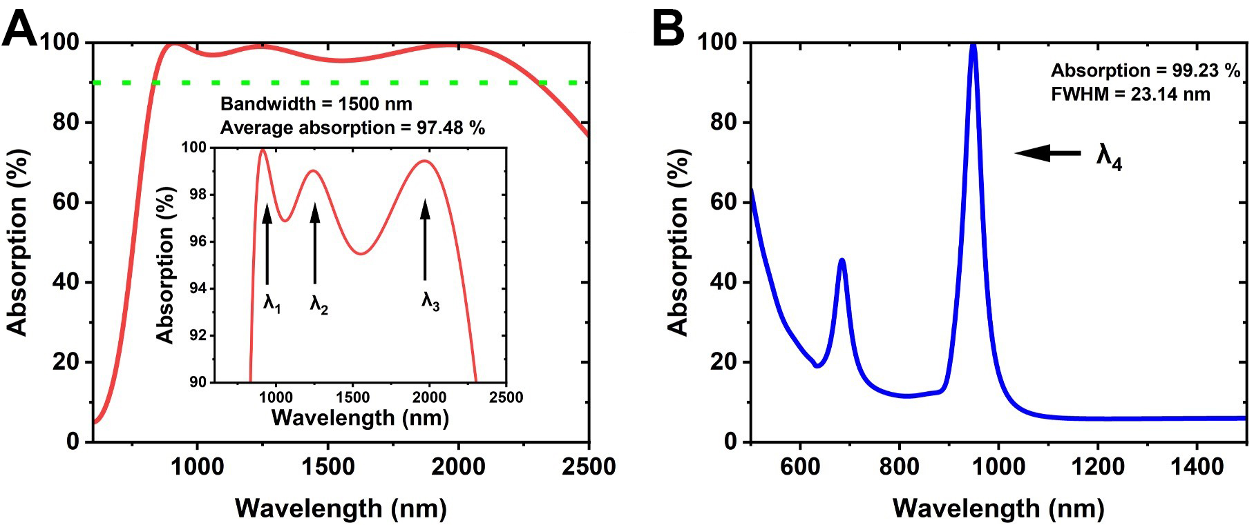
Figure 2. Broadband absorption spectrum (A) of the BMA with an average absorptivity of 97.48% over 800-2,300 nm for vertically incident light, the inset shows a magnified view of these three prominent absorption peaks. Narrowband absorption spectrum (B) of the BMA presents a near perfect absorption peak, with an absorptivity of 99.23% and a FWHM of 23.14 nm. BMA: Bifunctional metamaterial absorber; FWHM: full width at half maximum.
where λmax and λmin denote the maximum and minimum values of the operating wavelength, respectively. Based on calculation, the proposed BMA achieves an average absorptivity of 97.48% over the wavelength range of 800-2,300 nm. In contrast, excitation of the BMA’s four-by-four square-grid array produces a narrowband absorption spectrum in Figure 2B with two prominent absorption peaks. The device exhibits a near-perfect absorptivity of 99.23% at 948.1 nm with a narrow full width at half maximum (FWHM) of 23.14 nm. The combination of highly efficient broadband absorption and spectrally selective narrowband absorption positions the BMA as a competitive candidate for multifunctional electromagnetic wave manipulation.
Near-field electric distributions
To elucidate the physical mechanisms underlying the broadband and narrowband absorption, we calculated the near-field distributions at the resonance wavelengths. A frequency-domain power monitor was employed to collect the electric field distributions and electric field vector maps on the top surface (xy plane) and at the central cross-section (xz plane). The narrowband and broadband modes exhibit distinct electromagnetic field distributions and electric field vector maps in Figures 3 and 4, reflecting the distinct coupling mechanisms of each mode. For the narrowband mode, the electric field intensity on the top surface at 948.1 nm is concentrated primarily at four corner edges of the ZrN square-grid array, as shown in Figure 3A. This field localization arises from the strong plasmonic confinement associated with localized surface plasmon resonances (LSPRs) in ZrN. The z-component of the electric field (EZ) in Figure 3C exhibits an antisymmetric distribution. The cross-sectional field profile in Figure 3E displays a symmetric distribution and extends above the ZrN square-grid array. This pattern is indicative of surface plasmon polariton (SPP) excitation and Rayleigh Anomalies (RAs) characteristics. In addition, the corresponding EZ distribution at the cross-section in Figure 3G also exhibits an antisymmetric field pattern whose intensity decays gradually away from the surface. These observations indicate that the narrowband perfect absorption is governed by hybrid couplings among RAs, SPPs, LSPRs, and surface multipole resonance modes. This absorption is driven by the interaction between the incident light and the top surface of the ZrN four-by-four square-grid array.
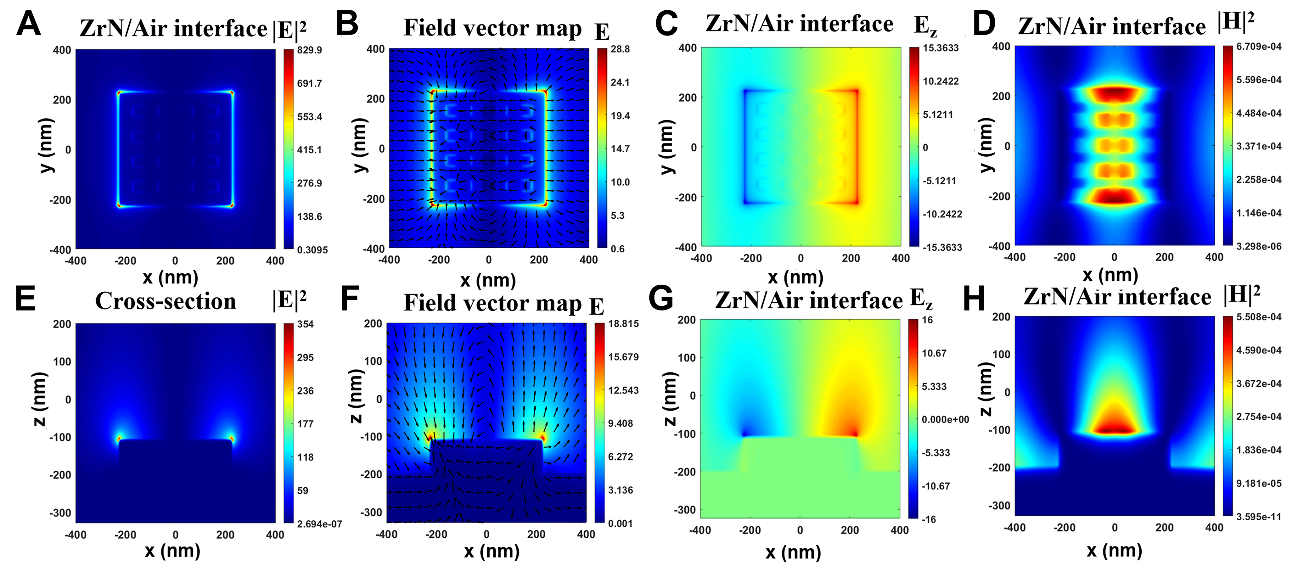
Figure 3. Electric field distributions (A) at the narrowband resonance wavelength on the top surface in xy plane and (E) at the cross-section in xz plane of the BMA, electric field vector maps (B and F), magnetic field distributions (D and H), and the corresponding EZ component (C and G) on the top surface and at the cross-section. BMA: Bifunctional metamaterial absorber; xz plane: central cross-section; xy plane: top surface; EZ: z-component of the electric field.
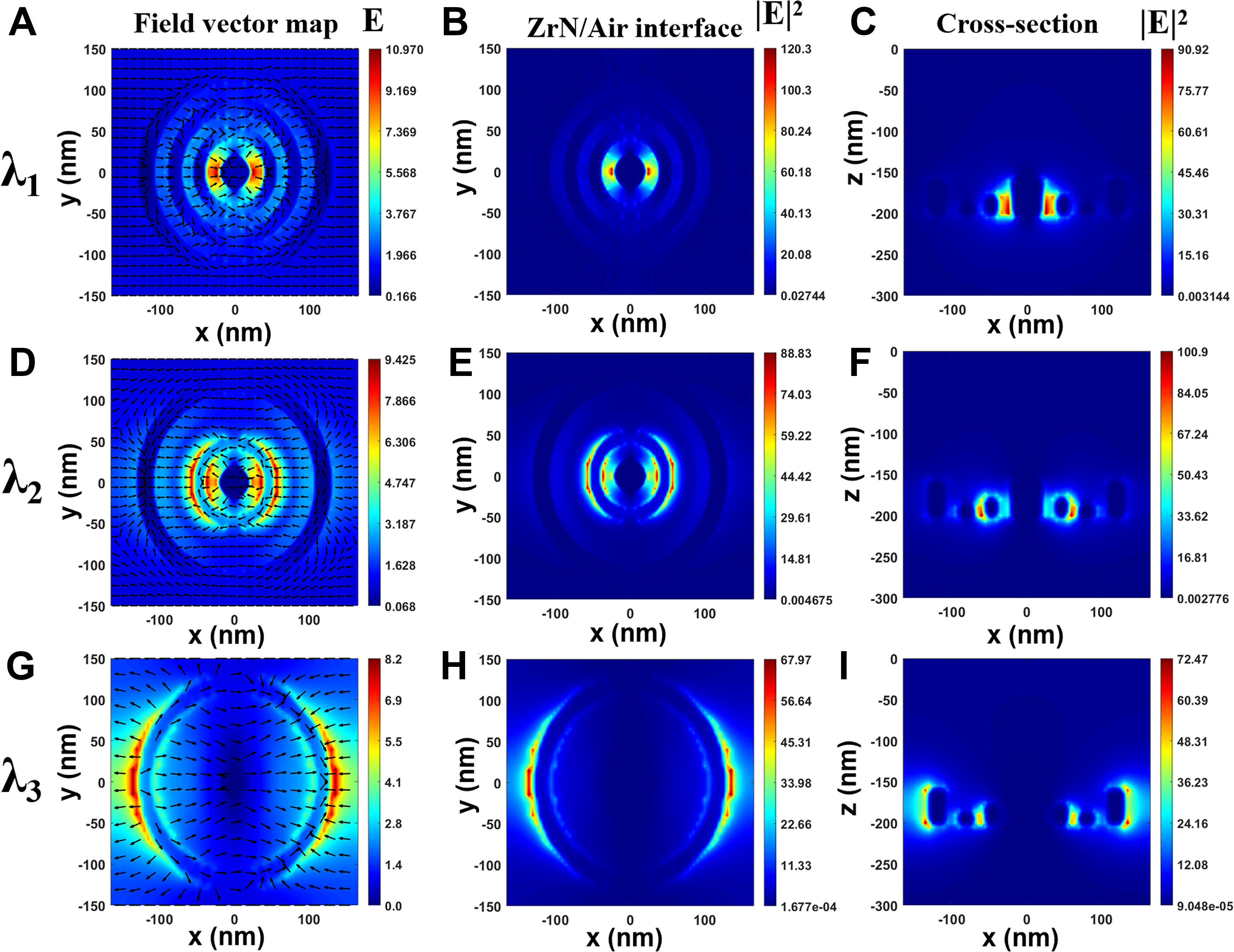
Figure 4. Electric field distributions (B, E and H) on the top surface in xy plane and (C, F and I) the cross-section in xz plane of the broadband absorption, and the electric field vector maps (A, D and G) at resonances of λ1, λ2, and λ3. ZrN: Zirconium nitride; xz plane: central cross-section; xy plane: top surface.
To further reveal the localized resonances of narrowband absorption, electric field vector maps reflecting the contributions of multipole moments are presented in Figure 3B and F. The vector maps reveal closed-loop current pathways at the top surface. Each current loop corresponds to an electric dipole (ED) mode. At the edges of the square grid array along the x-direction, a magnetic dipole (MD) response also appears. These features suggest that the narrowband resonance arises primarily from the coupled MD and ED modes. Meanwhile, the current loops observed within the small square holes in Figure 3B imply the participation of weak higher-order multipolar components. This interpretation is corroborated by the multipole decomposition analysis in Supplementary Figure 3A, which confirms that the resonance near 948.1 nm is dominated by ED and MD modes. As revealed by the magnetic fields in Figure 3D and H, the main MD mode is accompanied by high-order moment components, further confirming the involvement of magnetic dipole and quadrupole moments in the enhanced resonances. For the mechanism of broadband perfect absorption, electric field distributions on the top surface and in the cross-section of the BMA’s concentric rings at wavelengths λ1, λ2, and λ3 [Figure 2A] are calculated and displayed in Figure 4B, C, E, F, H and I. Clearly, the electric field and electric vector map on the xy plane at λ1 [Figure 4A and B] are intensively focused on the edge of the central disc, representing a typical electric dipole mode. As revealed by the cross-section profiles in Figure 4C, the field is mainly confined within the first ring gap, indicating strong LSPRs between the central ZrN disc and the first ring. At the resonance wavelength λ2, the field is mainly distributed between the second and third rings [Figure 4E and F]. This distribution indicates a strong plasmonic hybridization gap resonance. This gap resonance is further enhanced by relatively smaller thickness of the middle ring. The electric vector map [Figure 4D] reveals closed-loop current pathways in the third ring gap, which indicate MD and ED modes.
Figure 4H and I further indicate the strong localized surface plasmon resonances concentrated at the edge of the outer ring dominating the broadband perfect absorption at λ3. This behavior arises from the combination of ED mode and the closed-loop-current-induced MD mode in Figure 4G. Therefore, the broadband absorption arises from three distinct mechanisms. At λ1, multipole resonance modes within the first ring dominate. At λ2, plasmonic hybridization gap interactions between the first and second rings are responsible. At λ3, LSPRs are concentrated on the edge of the outer ZrN ring. This interpretation is further verified by the multipole decomposition analysis in Supplementary Figure 3B. The analysis confirms that the broadband response is dominated by the ED contribution, with additional MD and weak EQ contributions over the operating wavelength range. To quantitatively corroborate the physical mechanisms revealed by the near-field distributions, a detailed layer-resolved absorption analysis is presented in Supplementary Figure 4 and Supplementary Table 4. These results indicate that the absorbed power is mainly localized in ZrN for both the broadband and narrowband absorption modes. Moreover, this concentric-ring architecture is constructed from an isotropic material, and its inherent rotational symmetry allows it to support multiple resonant modes over a wide wavelength range. Under normal incidence, this symmetry also ensures polarization-insensitive absorption.
Structural parameters optimization
To examine the influence of different geometric parameters on the broadband absorption performance, we conducted a detailed parametric study of the ZrN concentric rings. Specifically, the inner radius (R) and the thickness (h) of the BMA are varied while maintaining Px = 330 nm and Py = 300 nm. Curves in Figure 5 reveal significant correlations rather than simple linear trends between the absorption properties and structural variations. Figs. 5(a)-(d) demonstrate that the average absorption of the BMA exhibits non-monotonic behavior with increasing ring thicknesses (h1, h2, h3, h4). The average absorptivity initially increases and then declines, reaching a maximum of 97.48% at h1 = 40 nm, h2 = 20 nm, and h4 = 40 nm, whereas the absorption decreases monotonically with increasing h3. The optimal average absorption is achieved with a set of thicknesses: h1 = 40 nm, h2 = 20 nm, h3 = 10 nm, and h4 = 40 nm. Similarly, increasing the BMA’s concentric ring radii (R1, R2 and R3) leads to an initial increase followed by a decrease in the average absorption [Figure 5E-G]. This trend is consistent with the results of the ring thickness in Figure 5A, B and 5D. This phenomenon can be attributed to the structural variations altering the air gaps between the adjacent rings, thereby modulating the electromagnetic resonance coupling. In addition, the role of the dielectric spacer in this absorber is investigated in Figure 5H. The absorption spectra exhibit an obvious redshift as the dielectric layer thickness increases. The average absorptivity first increases and then decreases, yielding a maximum average absorptivity of 97.48% at hSiO2 = 170 nm. These results suggest that optimized average absorption can be achieved across the 500-2,500 nm range through the combinations of appropriate parameters. The parameter-dependent trends further clarify the physical origin of the broadband absorption. Specifically, the ring dimensions determine the spectral positions of the resonant modes by modifying the effective current path and the localized electric response of each ring. The gaps between adjacent rings control the near-field coupling and plasmonic hybridization strength, thereby ruling the interaction and spectral overlap between neighboring resonances. In addition, the SiO2 spacer thickness regulates the couplings between the ZrN concentric-ring resonators, which affects the effective magnetic response and the overall impedance-matching condition.
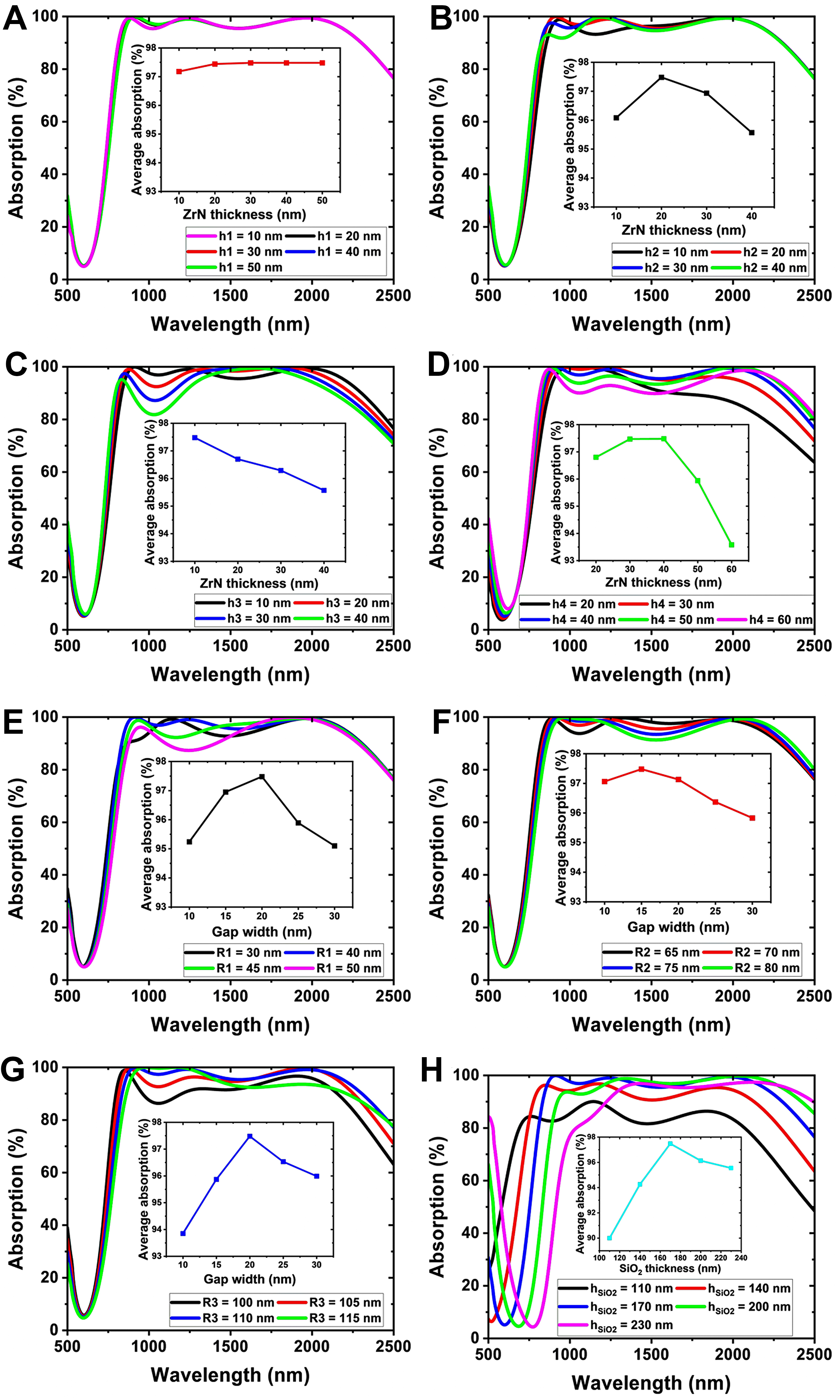
Figure 5. Simulated broadband absorption spectra of the BMA based on ZrN under vertical incidence demonstrate the effects of fixed parameters on optical performance: ring thickness variation with fixed parameters of h1 = 40 nm (A), h2 = 20 nm (B), h3 = 10 nm (C), and h4 = 40 nm (D); ring radius variation with R1 = 40 nm (E), R2 = 70 nm (F) and R3 = 110 nm (G); and SiO2 spacer layer thickness variation with hSiO2 = 170 nm (H). The insets illustrate the corresponding average absorption changes as a function of parameter variation. BMA: Bifunctional metamaterial absorber; ZrN: zirconium nitride.
Apart from the influence of structural parameter variations on broadband absorption properties, effects of the structural parameters of the four-by-four square grid array on the narrowband absorption are also studied. The optical response of the BMA depends not only on the geometric parameters of the meta-atoms but also significantly on the physical dimensions. The formation of RAs under vertical incidence on a metasurface is primarily determined by its periodicity, as expressed in the following equation[34]:
where n represents the refractive index of the surrounding medium, and (i, j) denotes the diffraction order of the RAs. The initial ranges of Px and Py were determined according to the subwavelength condition in the investigated spectral range and considerations of fabrication feasibility. Based on these ranges, the absorption spectra were calculated for a systematic set of Px and Py values to assess the influence of periodicity on the absorption performance. Figure 6A shows the absorption spectra obtained by varying Px under normal incidence, together with the curves of the (±1, 0)- and (±1, ±1)-order RAs. The resonance wavelengths exhibit an obvious redshift as Px increases. Notably, λ4 almost coincides with the (±1, 0)-order RA curves, indicating that the degenerate (+1, 0) and (-1, 0) RAs collectively contribute to the resonance. This suggests a hybridization between localized multipolar resonances and lattice diffraction RA modes, enabling stronger in-plane field confinement and narrowband absorption.
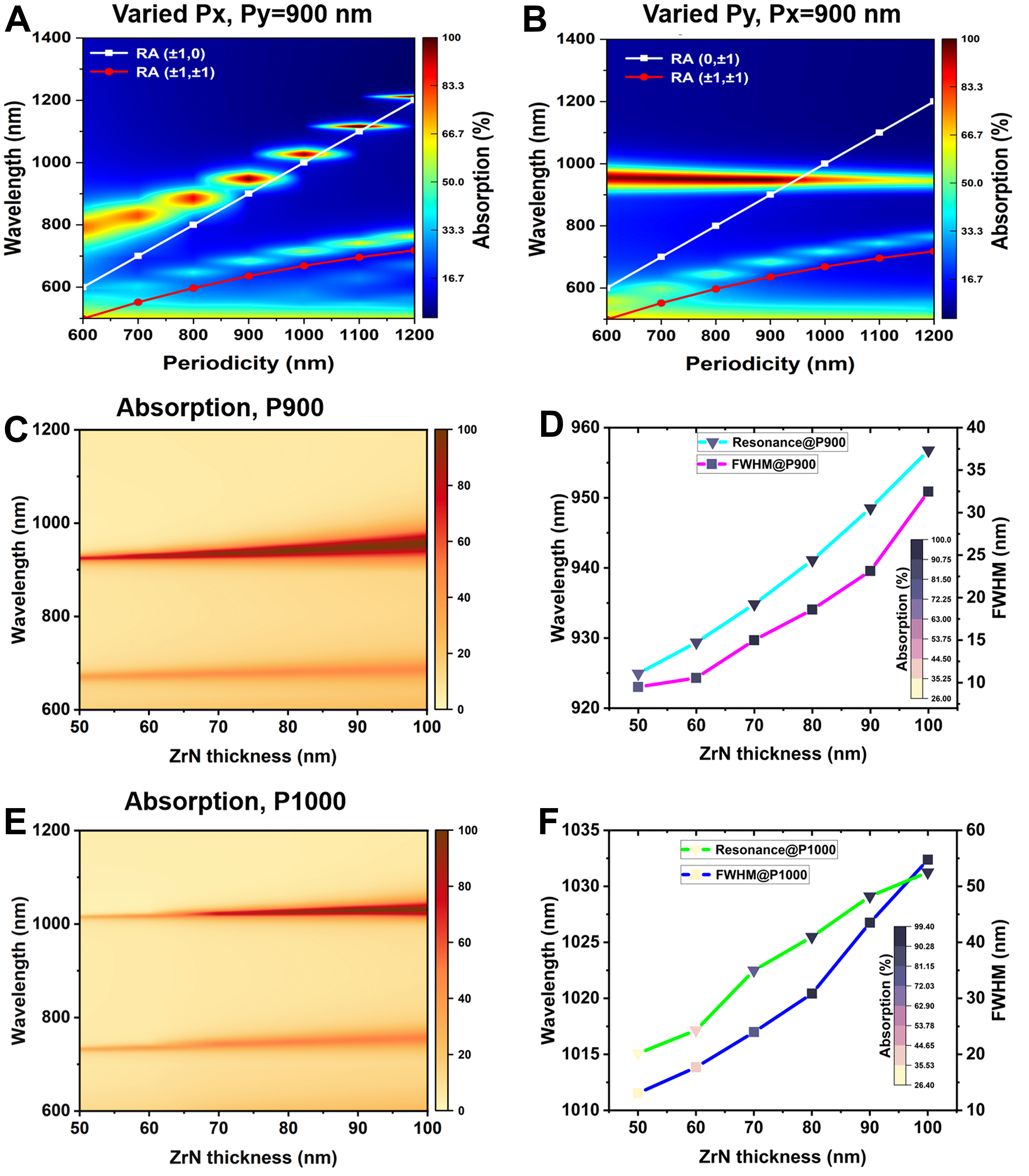
Figure 6. Narrowband absorption spectra of BMA with parameters: hZrN = 80 nm, L = 400 nm and W = 50 nm, obtained by varying Px (A) and Py (B) under vertical incidence while keeping the other periodic component equal to 900 nm with the inset curves of (0, ±1)-, (±1, 0)- , and (±1, ±1)-order RAs, variation of the ZrN thickness effects on the absorptivity and the FWHM for periods of 900 nm (C and D) and 1,000 nm (E and F). ZrN: Zirconium nitride; BMA: bifunctional metamaterial absorber; RA: Rayleigh Anomalie; FWHM: full width at half maximum.
Figure 6B presents the spectra obtained by varying Py while keeping Px = 900 nm. In this case, λ4 exhibits almost no redshift, indicating that varying Py has a much weaker influence on the resonance position. Near-perfect narrowband spectra can therefore be achieved for both Px = Py = 900 and Px = Py = 1000 nm. The corresponding quality factors for periodicities of 900 and 1,000 nm are 73.49 and 73.89, respectively. Figure 6C shows the effect of ZrN thickness on the absorptivity for the periodicity of 900 nm, while Figure 6D gives the corresponding variation in the FWHM. Similarly, Figure 6E displays the absorptivity for the periodicity of 1,000 nm, and Figure 6F displays the corresponding FWHM variation. The absorption spectra become broader and the resonance peaks exhibit a redshift as the ZrN thickness increases, implying an increasing trend in the FWHM. The optimal performance is obtained at the periodicity of 900 nm with hZrN = 90 nm, yielding a near-perfect absorptivity of 99.23% and a narrow FWHM of 23.14 nm. These results confirm that the careful optimization of structural parameters is essential for achieving optimal narrowband spectral performance. Given this sensitivity to geometric precision, we present a rigorous dimensional tolerance analysis in Supplementary Figure 5 and 6 and Supplementary Tables 5 and 6 to assess the fabrication feasibility of the proposed BMA.
Impedance matching
Impedance matching theory provides additional insight into the absorption performance of the ZrN-based metamaterial in both broadband and narrowband regimes. According to Equation 6[35], the relative impedance Zr of the BMA can be calculated from the scattering parameters as follows:
where S11 and S21 are the scattering parameters. Generally, the resonance impedance of an absorber is governed by its geometry configuration and the intrinsic electromagnetic properties of its constituent materials. The proposed BMA, which comprises a ZrN-based periodic nanostructure, can be treated as an effective homogeneous medium. Its electromagnetic response is then fully described by the complex relative permittivity ε(ω) = ε0εr and relative permeability µ(ω) = µ0 µr.
These parameters collectively determine the metamaterial impedance
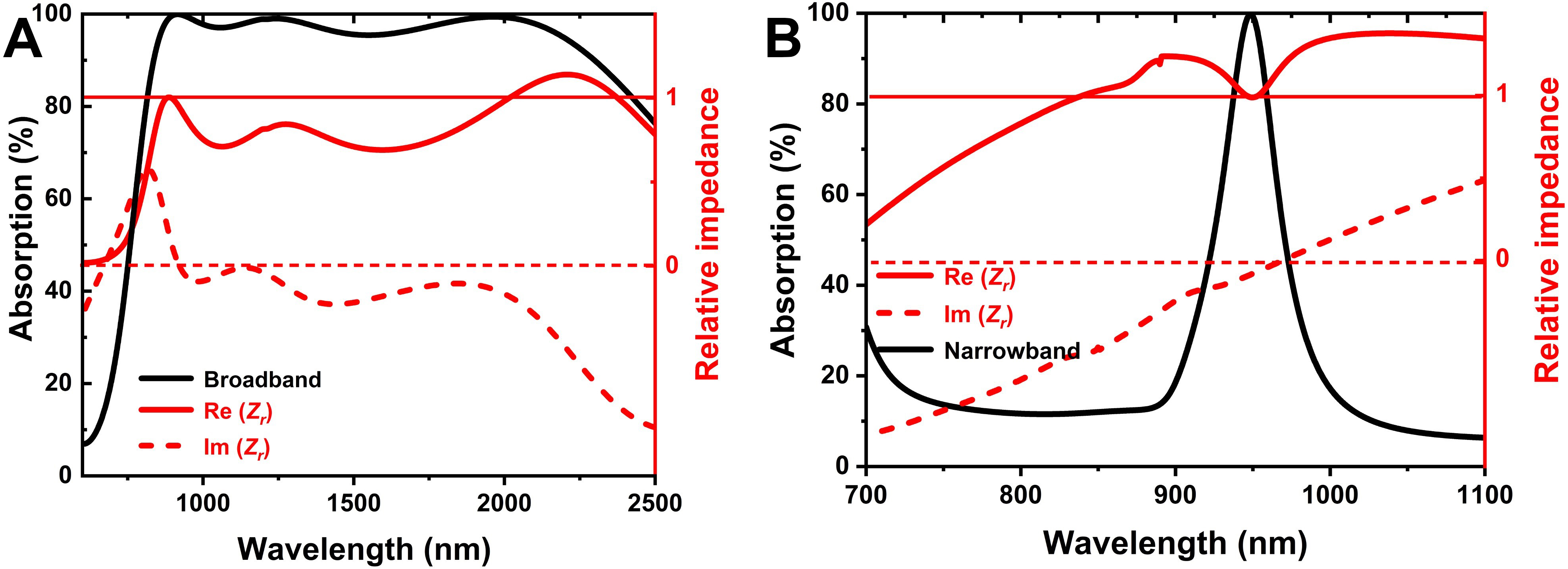
Figure 7. The corresponding relative impedance response of broadband absorption (A) and narrowband absorption (B), where the left axis represents the absorption spectra, while the right axis displays the relative impedance of the metamaterial: real part Re(Zr) (solid red line) and imaginary part Im(Zr) (dashed red line).
Polarization and incidence angle independence
When considering solar thermophotovoltaic applications in complex electromagnetic environments, an absorber with polarization- and incidence-angle-insensitive features is preferred. We therefore investigated the influence of polarization and incidence angle on broadband absorption properties of the BMA. Under transverse electric (TE) polarization [Figure 8A], the absorption spectra maintain a relatively high absorptivity but undergo a slight blueshift as the incidence angle (θ) increases. The corresponding calculated average absorption slightly decreases from 97.48% at an incidence angle of 0° to 86.32% at 50°. Under transverse magnetic (TM)-polarization [Figure 8B], the broadband absorption bandwidth gradually narrows as incidence angle increases, although the absorption spectra remain almost unchanged. The average absorptivity still reaches a relatively high level of 94.86% at an incidence angle of 50°. The in-plane symmetry of the concentric-ring geometry ensures polarization-insensitivity under normal incidence. Under oblique incidence, however, TE and TM waves are no longer equivalent. Their wave impedances and field-component distributions differ, which produces distinct impedance-matching conditions for these two polarizations. Consequently, the absorptivity decreases rapidly for TE polarization as the incident angle increases, whereas TM polarization maintains stable absorption performance. These results demonstrate that the proposed BMA exhibits robust angular and polarization stability. The device is therefore suited for light harvesting under arbitrarily polarized and obliquely incident illumination.
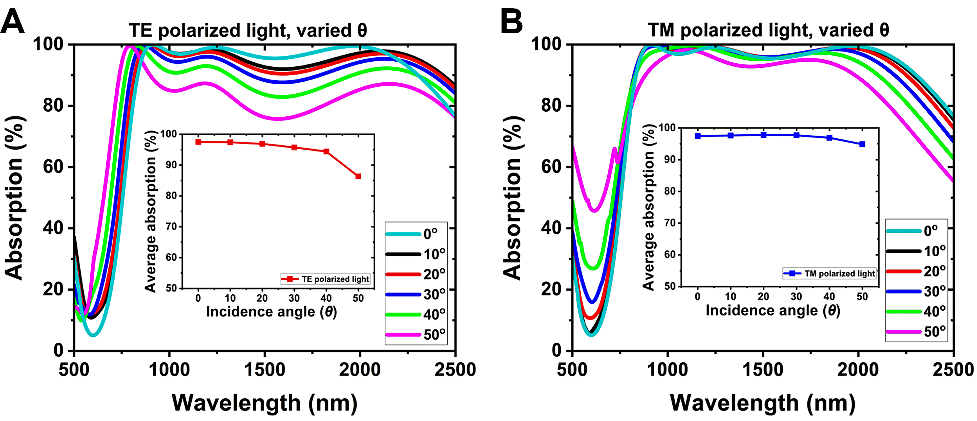
Figure 8. Absorption as a function of incidence angle (θ = 0°,10°,20°,30°,40°,50°) and wavelength for TE (A) and TM (B) polarizations. Insets show the absorption ratio with respect to incidence angle θ. TE: Transverse electric; TM: transverse magnetic.
Broadband absorption performance comparison
After a comprehensive investigation of the BMA’s broadband absorption properties, comparison between the designed concentric-ring metamaterial and the absorbers reported in the literature is presented in Table 1. In terms of average absorptivity and operating bandwidth, our design exhibits a high absorptivity of 97.48% over the range from 800 to 2,300 nm, surpassing most reported absorbers[36-38]. This highlights the strong potential of the proposed design for broadband light harvesting.
Comparison of broadband absorption performance with reported works
| Ref. | Structure | Operation frequency | Average absorptivity | Broadband width |
| [14] | ZrN/SiO2/ZrN | 400-800 nm | 95 % | 400 nm |
| [23] | Au/SiO2/Ti/Si3N4 | 400-900 nm | 97.89 % | 500 nm |
| [36] | TiO2/Si | 820-1440 nm | > 90 % | 620 nm |
| [37] | Si/MgF4/Cr/ GaAs/SiO2 | 800-1800 nm | 96.3 % | 1,000 nm |
| [38] | Ti/SiO2/Au | 900-1825 nm | > 90 % | 925 nm |
| Our work | ZrN/SiO2/Au/ZrN | 800-2300 nm | 97.48 % | 1,500 nm |
Metamaterial emitter design
According to Kirchhoff’s law of thermal radiation, absorptivity equals emissivity under thermal equilibrium[39]. A selective absorber can therefore serve as a selective emitter when operated at a specific working temperature. Exploiting this principle, a thermophotovoltaic energy conversion system can be constructed using a structure consisting of an absorber and an emitter mounted between the incident solar radiation and a photovoltaic (PV) cell. This configuration optimizes solar energy utilization. In such system, the absorber collects broadband solar radiation and the emitter re-radiates it as selective narrowband emission spectrally matched with the bandgap of the PV cell.
The PV cell bandgap critically affects the conversion efficiency. PV cells with a wide bandgap cannot harvest the full solar spectrum, while those with low bandgaps waste most of the energy from high-energy photons through thermalization losses. To overcome this limitation, III-V multi-junction PV cells with an energy bandgap (Eg) ranging from 0.7 to 1.9 eV can achieve optimal conversion efficiencies > 94.51%[40]. For the proposed BMA, the emitter performance was investigated by varying the periodic dimensions [Figure 9] to assess the realization of different bandgap energies within the range of 0.7 to 1.9 eV, where most PV cells operate. The structural parameters of the emitter are: h1 = 40 nm, h2 = 20 nm, h3 = 10 nm, and h4 = 40 nm; R1 = 40 nm, R2 = 70 nm, R3 = 110 nm, r = 20 nm, hSiO2 = 170 nm, and hZrN = 90 nm. The emittance spectra obtained with a fixed Py = 300 nm and varied Px are shown in Fig. 9(a), while those obtained with a fixed Px = 300 nm and varied Py are displayed in Figure 9B. The average emittance value of each spectrum is calculated according to Equation 4 as shown by the insets in Figure 9A and B. Under TM-polarized excitation with Py fixed at 300 nm, the average emittance initially rises and then decreases as Px increases from 275 to 475 nm [Figure 9A]. The emittance reaches a maximum of 97.98% at Px = 375 nm, corresponding to the range of 0.7 to 1.5 eV. When Py is varied with Px fixed at 300 nm [Figure 9B], the extracted average emittance follows the same non-monotonic trend as in Figure 9A, although the peak levels are slightly lower. The maximum emittance of 96.46% is reached at Py = 325 nm. Although varying the periodicity of the BMA along the x-direction under TM polarization results in slightly higher average emittance values than varying along y-direction, both sets of calculated values demonstrate great emittance performance. This suggests that such a periodically arranged concentric-ring ZrN-based metamaterial can realize effective spectral matching with the bandgap of photovoltaic cells.
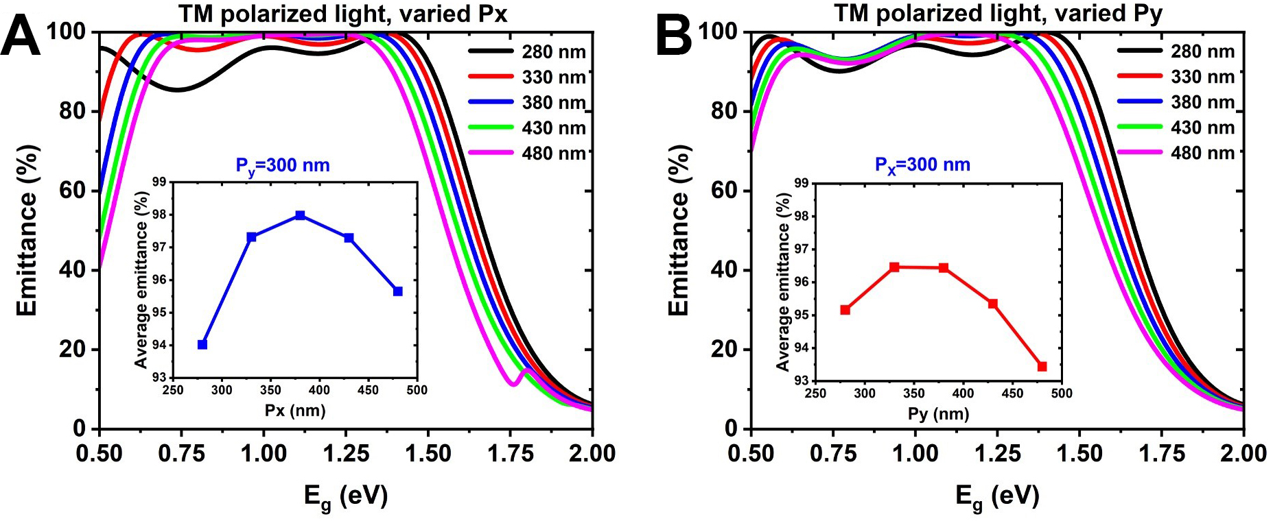
Figure 9. Emittance spectra of the BMA under TM-polarized light source as a function of energy bandgap (Eg) with variation of the periodic components along (A) x-direction and (B) y-direction while keeping the other periodic component fixed. TM: BMA: bifunctional metamaterial absorber.
Narrowband refractive index sensing
Narrowband absorbers with near-perfect absorption and narrow bandwidths have attracted attention for emission devices, biosensing, and related applications[18-21]. The spectral response arising from these light-matter interactions is sensitive to variations in the environmental refractive index. Herein, we investigated the refractive index sensing performance of the BMA’s narrowband absorption mode by varying the refractive index from 1.00 to 1.10 in steps of 0.02. The obtained reflectance spectra exhibit distinct redshifts with a similar wavelength shift of 20.34 nm in Figure 10A. Throughout this refractive index range, the absorptivity remains at near-perfect absorption level.
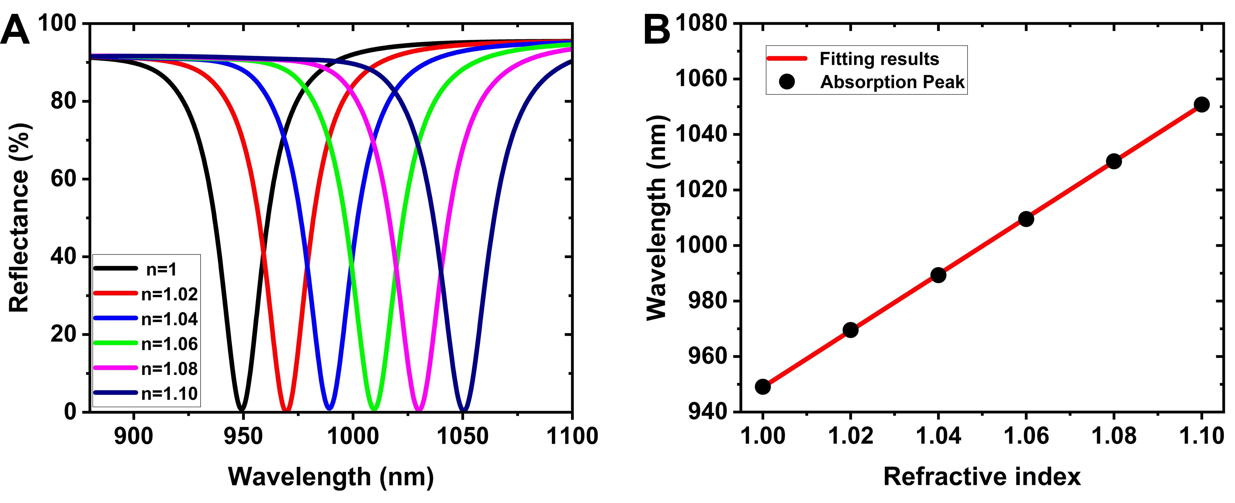
Figure 10. Narrowband reflection spectra (A) of the BMA under vertical incidence with TM polarization in superstrate with varied refractive indices; (B) the corresponding extracted resonance wavelengths as a function of the refractive index with a fitted linear relationship. BMA: Bifunctional metamaterial absorber; TM:
As shown in Figure 10B, the resonance wavelengths are extracted and fitted according to Equation 7 for the refractive index sensitivity (S):
where ∆λ and ∆n denote the resonance wavelength shift and the refractive index difference, respectively. The sensitivity is calculated to be 1,015.62 nm RIU-1. Derived from the sensitivity and FWHM, the deduced FOM is another important metric for evaluating sensing performance[34], as expressed by Equation 8.
The calculated FOM of the BMA is 44.15 RIU-1, outperforming several reported bifunctional absorbers, as listed in Table 2. The combination of high sensitivity and narrow spectral linewidth demonstrates that the ZrN-based four-by-four square-grid array is well suited for precision refractive index sensing. Potential application areas include advanced biosensing platforms and environmental monitoring systems, where high spectral resolution is required.
Comparison of the BMA’s sensitivity with some reported works
| Ref. | Structure | Resonance wavelength | Sensitivity | FOM |
| [41] | TiO2/SiO2/Au | 865.3 nm | 50 nm RIU-1 | 5 RIU-1 |
| [42] | Si/SiO2/Si | 510 nm | 300 nm RIU-1 | 2.0 RIU-1 |
| [43] | Graphene/SiO2/Au | 886 nm | 344 nm RIU-1 | 10.4 RIU-1 |
| [44] | Graphene/SiO2/Au | 1,611 nm | 430 nm RIU-1 | 4.4 RIU-1 |
| [23] | Au/SiO2/Ti/Si3N4 | 647 nm | 625 nm RIU-1 | 37 RIU-1 |
| Our work | ZrN/SiO2/Au/ZrN | 948.1 nm | 1,015.62 nm RIU-1 | 44.15 RIU-1 |
More importantly, our BMA achieves a broadband absorptivity of 97.48% over the wavelength range from 800 to 2,300 nm and a near-perfect narrowband absorptivity of 99.23% at 948.1 nm, with a refractive index sensitivity of 1,015.62 nm RIU-1. This performance significantly surpasses that of Gao’s bifunctional absorber, which delivers a broadband absorptivity of 84.09% over 400 to 900 nm, and a sensitivity of 625 nm RIU-1 at 647 nm with an absorptivity of 94.68%. This comparison indicates that our proposed BMA successfully integrates bifunctionality within a single device. It simultaneously delivers high absorption efficiency over ultra-broadband operation wavelengths, and competitive narrowband refractive index sensitivity, establishing a promising platform for energy harvesting, bio-detection, sensing technologies, and environmental monitoring.
CONCLUSIONS
In summary, a bifunctional ZrN-based metamaterial absorber integrating broadband and narrowband absorption within a single device has been numerically demonstrated in the visible to near-infrared range. The proposed BMA achieves an average absorptivity of 97.48% over 800-2,300 nm for broadband absorption, and a near-perfect narrowband absorptivity of 99.23% at 948.1 nm with a FWHM of 23.14 nm. In addition, the narrowband mode exhibits a high refractive index sensitivity of 1,015.62 nm RIU-1 and a FOM of 44.15 RIU-1, emphasizing its promising sensing capability. Near-field distributions and impedance analyses reveal that the absorption performance arises from the hybrid couplings of LSPRs, SPPs, RAs-assisted coupling, and multipole resonance modes. Owing to the thermal and chemical stability of ZrN and the relatively robust broadband absorption maintained under oblique incidence, the proposed design demonstrates significant potential for applications in energy harvesting and biosensing. However, since the present design is passive and geometrically fixed after fabrication, future work would explore tunable materials or reconfigurable architectures to realize dynamic control and further expand the scope of applications.
DECLARATIONS
Authors’ contributions
Methodology: Zuo, Y.; Han, W.
Validation: Zuo, Y.
Formal analysis: Zuo, Y.; Han, W.; Wei, G.; Liu, Y.; Wang, S.
Writing - original draft: Zuo, Y.; Han, W.
Conceptualization: Han, W.
Funding Acquisition: Han, W.; Du, K.; Wang, S.
Writing - review & editing: Han, W.
Software: Wei, G.
Validation: Du, K.; Liu, Y.
Resources: Wang, S.
Availability of data and materials
The original contributions presented in this study are included in the article/Supplementary Materials. Further inquiries can be directed to the corresponding authors.
AI and AI-assisted tools statement
Not applicable.
Financial support and sponsorship
This work was supported by the National Natural Science Foundation of China (No. 52402153), the Natural Science Foundation of Hubei Province (No. 2024AFB888), and the Foundation of Wuhan Textile University (No. 243061).
Conflicts of interest
All authors declared that there are no conflicts of interest.
Ethical approval and consent to participate
Not applicable.
Consent for publication
Not applicable.
Copyright
© The Author(s) 2026.
Supplementary Materials
REFERENCES
1. Esfandiari, M.; Lalbakhsh, A.; Nasiri Shehni, P.; et al. Recent and emerging applications of Graphene-based metamaterials in electromagnetics. Mater. Des. 2022, 221, 110920.
2. Zhou, R.; Wang, Y.; Liu, Z.; Pang, Y.; Chen, J.; Kong, J. Digital light processing 3D-printed ceramic metamaterials for electromagnetic wave absorption. Nano-Micro. Lett. 2022, 14, 122.
3. Gao, N.; Zhang, Z.; Deng, J.; Guo, X.; Cheng, B.; Hou, H. Acoustic metamaterials for noise reduction: a review. Adv. Mater. Technol. 2022, 7, 2100698.
4. Krushynska, A. O.; Torrent, D.; Aragón, A. M.; et al. Emerging topics in nanophononics and elastic, acoustic, and mechanical metamaterials: an overview. Nanophotonics 2023, 12, 659-86.
5. Jiao, P.; Mueller, J.; Raney, J. R.; Zheng, X.; Alavi, A. H. Mechanical metamaterials and beyond. Nat. Commun. 2023, 14, 6004.
6. Deng, B.; Zareei, A.; Ding, X.; Weaver, J. C.; Rycroft, C. H.; Bertoldi, K. Inverse design of mechanical metamaterials with target nonlinear response via a neural accelerated evolution strategy. Adv. Mater. 2022, 34, 2206238.
7. Landy, N. I.; Sajuyigbe, S.; Mock, J. J.; Smith, D. R.; Padilla, W. J. Perfect metamaterial absorber. Phys. Rev. Lett. 2008, 100, 207402.
9. Metamaterials: Theory, Design, and Applications; Cui, T. J., Smith, D., Liu, R., Eds.; Springer US, 2010.
10. Wu, F.; She, Y.; Zhou, T.; Cheng, Z.; Huang, J. Hybrid one-dimensional photonic crystals containing anisotropic metamaterials: angle-driven photonic band gaps and angle-driven Tamm plasmon polaritons. Phys. Rev. A. 2024, 110, 023503.
11. Cummer, S. A.; Christensen, J.; Alù, A. Controlling sound with acoustic metamaterials. Nat. Rev. Mater. 2016, 1, 16001.
12. Jang, E.; Cho, J.; Kang, C.; Chung, H. Inverse design of ultrathin metamaterial absorber. Nanomaterials 2025, 15, 1024.
13. Song, Z.; Zhang, R.; Min, P.; et al. Inverse design of diffusion-absorption hybrid metasurfaces. Laser. Photonics. Rev. 2023, 17, 2300280.
14. Ijaz, S.; Rana, A. S.; Ahmad, Z.; Rehman, B.; Zubair, M.; Mehmood, M. Q. Exploiting zirconium nitride for an efficient heat-resistant absorber and emitter pair for solar thermophotovoltaic systems. Opt. Express. 2021, 29, 31537.
15. Wu, S.; Wu, T.; Xiong, G. Ultra-broadband high solar absorption in checkerboard-shaped titanium nitride plasmonic metastructures. Opt. Mater. 2021, 116, 111117.
16. Huang, S.; Chen, Y.; Yu, C.; et al. Optimized metamaterial solar absorber with ultra-wideband, polarization-independent and large incident angle-insensitive. Chin. J. Phys. 2024, 89, 740-7.
17. Wang, Y.-X.; Zhang, Y.; Du, L.; Wu, J.-H. Chiral phase modulation and a tunable broadband perfect absorber using a coherent cold atomic ensemble. Phys. Rev. A. 2023, 108, 053716.
18. Jung, J.; Lee, J.; Choi, J.; Choi, D.; Jeong, J. Enhancement of refractive index sensing for an infrared plasmonic metamaterial absorber with a nanogap. Opt. Express. 2021, 29, 22796.
19. Higgins, S. G.; Becce, M.; Belessiotis‐richards, A.; Seong, H.; Sero, J. E.; Stevens, M. M. High-aspect-ratio nanostructured surfaces as biological metamaterials. Adv. Mater. 2020, 32, 1903862.
20. Watts, C. M.; Liu, X.; Padilla, W. J. Metamaterial electromagnetic wave absorbers. Adv. Mater. 2012, 24. , OP98-120, OP181.
21. Liu, X.; Starr, T.; Starr, A. F.; Padilla, W. J. Infrared spatial and frequency selective metamaterial with near-unity absorbance. Phys. Rev. Lett. 2010, 104, 207403.
22. Kang, S.; Qian, Z.; Rajaram, V.; Calisgan, S. D.; Alù, A.; Rinaldi, M. Ultra-narrowband metamaterial absorbers for high spectral resolution infrared spectroscopy. Adv. Opt. Mater. 2018, 7, 1801236.
23. Gao, H.; Liang, Y.; Yu, L.; et al. Bifunctional plasmonic metamaterial absorber for narrowband sensing detection and broadband optical absorption. Opt. Laser. Technol. 2021, 137, 106807.
24. Li, J.; Chen, Z.; Yang, H.; et al. Tunable broadband solar energy absorber based on monolayer transition metal dichalcogenides materials using Au nanocubes. Nanomaterials 2020, 10, 257.
25. Zhang, S.; Li, Y.; Feng, G.; et al. Strong infrared absorber: surface-microstructured Au film replicated from black silicon. Opt. Express. 2011, 19, 20462.
26. Günaydın, B. N.; Gülmez, M.; Torabfam, M.; et al. Plasmonic titanium nitride nanohole arrays for refractometric sensing. ACS. Appl. Nano. Mater. 2023, 6, 20612-22.
27. Benia, H.; Guemmaz, M.; Schmerber, G.; Mosser, A.; Parlebas, J. Optical and electrical properties of sputtered ZrN compounds. Catal. Today. 2004, 89, 307-12.
28. Hansen, K.; Dutta, A.; Cardona, M.; Yang, C. Zirconium nitride for plasmonic cloaking of visible nanowire photodetectors. Plasmonics 2020, 15, 1231-41.
29. Pilloud, D.; Dehlinger, A.; Pierson, J.; Roman, A.; Pichon, L. Reactively sputtered zirconium nitride coatings: structural, mechanical, optical and electrical characteristics. Surf. Coat. Technol. 2003, 174-175, 338-44.
30. Diroll, B. T.; Saha, S.; Shalaev, V. M.; Boltasseva, A.; Schaller, R. D. Broadband ultrafast dynamics of refractory metals: TiN and ZrN. Adv. Opt. Mater. 2020, 8, 2000652.
31. Rahad, R.; Haque, M. A.; Mahadi, M. K.; et al. Highly sensitive optically tunable transition metal nitride-based plasmonic pressure sensor with CMOS-compatibility at compact subwavelength dimensions. IEEE. Sensors. J. 2024, 24, 22271-8.
32. Naik, G. V.; Shalaev, V. M.; Boltasseva, A. Alternative plasmonic materials: beyond gold and silver. Adv. Mater. 2013, 25, 3264-94.
33. Yan, X.; Lin, Q.; Wang, L.; Liu, G. Active absorption modulation by employing strong coupling between magnetic plasmons and borophene surface plasmons in the telecommunication band. J. Appl. Phys. 2022, 132, 063101.
34. Han, W.; Zuo, Y.; Wei, G.; et al. Tunable ultra-narrow multi-band anisotropic metamaterial perfect absorbers based on α-phase molybdenum trioxide for refractive index sensing application. Measurement 2026, 261, 119881.
35. Smith, D. R.; Vier, D. C.; Koschny, T.; Soukoulis, C. M. Electromagnetic parameter retrieval from inhomogeneous metamaterials. Phys. Rev. E. 2005, 71, 036617.
36. Zhu, Y.; Lan, T.; Liu, P.; Yang, J. Broadband near-infrared TiO2 dielectric metamaterial absorbers. Appl. Opt. 2019, 58, 7134.
37. Wang, Y.; Liu, Z.; Zhou, F.; Yi, Z.; Wang, J. Perfect absorption properties of a near-infrared super-surface perfect absorber based on a multilayer subwavelength array structure. Phys. Lett. A. 2025, 540, 130395.
38. Ding, F.; Dai, J.; Chen, Y.; Zhu, J.; Jin, Y.; Bozhevolnyi, S. I. Broadband near-infrared metamaterial absorbers utilizing highly lossy metals. Sci. Rep. 2016, 6, 39445.
39. Chang, C.; Kort-kamp, W. J. M.; Nogan, J.; et al. High-temperature refractory metasurfaces for solar thermophotovoltaic energy harvesting. Nano. Lett. 2018, 18, 7665-73.
40. Friedman, D.; Geisz, J.; Norman, A.; Wanlass, M.; Kurtz, S. 0.7-eV GaInAs Junction for a GaInP/GaAs/GaInAs(1eV)/GaInAs(0.7eV) Four-Junction Solar Cell. In 2006 IEEE 4th World Conference on Photovoltaic Energy Conference, Waikoloa, HI, May 7-12, 2006; IEEE, 2006, pp 598-602.
41. Liu, B.; Wu, P.; Zhu, H.; Lv, L. Ultra narrow dual-band perfect absorber based on a dielectric-dielectric-metal three-layer film material. Micromachines 2021, 12, 1552.
42. Khonina, S. N.; Butt, M. A.; Kazanskiy, N. L. Numerical investigation of metasurface narrowband perfect absorber and a plasmonic sensor for a near-infrared wavelength range. J. Opt. 2021, 23, 065102.
43. Li, R.; Zheng, Y.; Luo, Y.; et al. Multi-peak narrow-band perfect absorber based on two-dimensional graphene array. Diamond. Relat. Mater. 2021, 120, 108666.
Cite This Article
How to Cite
Download Citation
Export Citation File:
Type of Import
Tips on Downloading Citation
Citation Manager File Format
Type of Import
Direct Import: When the Direct Import option is selected (the default state), a dialogue box will give you the option to Save or Open the downloaded citation data. Choosing Open will either launch your citation manager or give you a choice of applications with which to use the metadata. The Save option saves the file locally for later use.
Indirect Import: When the Indirect Import option is selected, the metadata is displayed and may be copied and pasted as needed.
About This Article
Special Topic
Copyright

Data & Comments
Data
0


Comments
Comments must be written in English. Spam, offensive content, impersonation, and private information will not be permitted. If any comment is reported and identified as inappropriate content by OAE staff, the comment will be removed without notice. If you have any queries or need any help, please contact us at [email protected].