


fig1
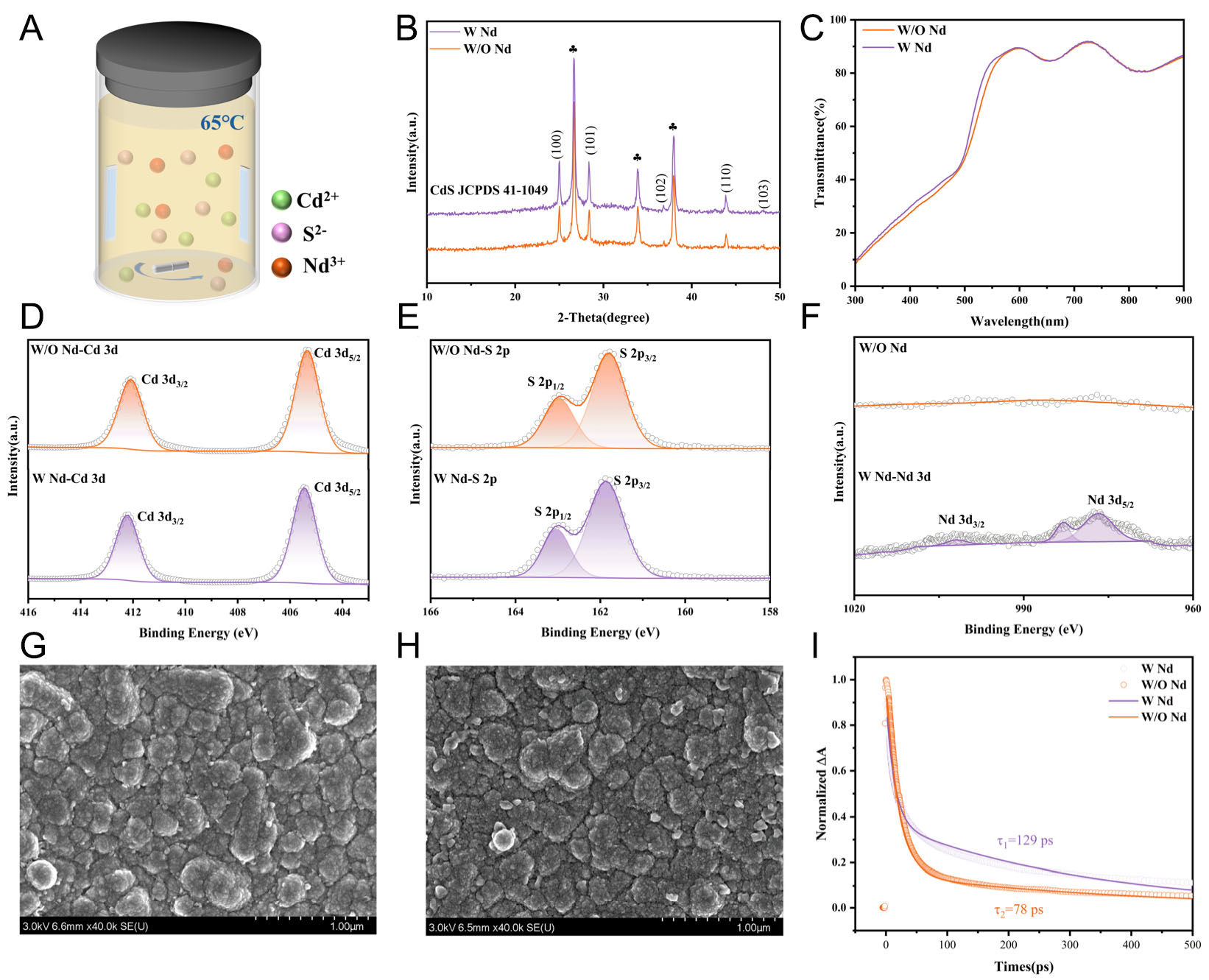
Figure 1. (A) Schematic diagram illustrating the deposition of Nd-incorporated CdS thin films, (B) XRD patterns of W Nd-CdS and W/O Nd-CdS samples, (C) Transmittance spectra, (D-F) XPS spectra of Cd 3d, S 2p, and Nd 3d, (G and H) Surface SEM images of W Nd-CdS and W/O Nd-CdS samples, (I) TAS spectra of W Nd-CdS and W/O Nd-CdS samples.


