

fig2
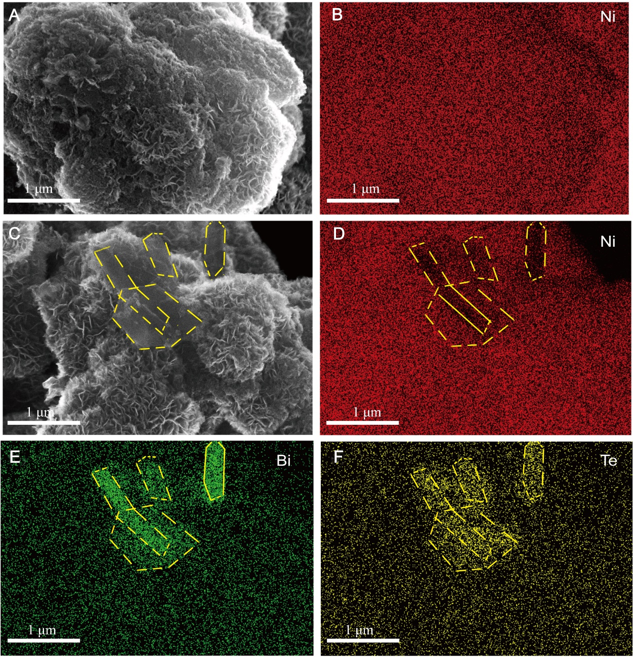
Figure 2. (A) Top-view SEM image of NiOx and (B) the corresponding Ni EDS mapping; (C) SEM image of 10% Bi2Te3@NiOx and the corresponding EDS mappings for (D) Ni, (E) Bi, and (F) Te. The yellow dashed box highlights a Bi2Te3-dominated area. SEM: Scanning electron microscope; EDS: energy-dispersive X-ray spectroscopy.