


Recent advances in zero-power optoelectronic synapses with potential for wearable neuromorphic platforms
 0
0 
Abstract
Zero-power optoelectronic synapses, defined as optoelectronic synaptic devices operating without external electrical bias, are emerging as core components for energy-efficient intelligent wearable neuromorphic platforms. Wearable neuromorphic systems require continuous, autonomous operation under strict constraints on power consumption, mechanical compliance, and thermal safety, making conventional electrically biased synaptic devices impractical for long-term body-interfaced use. By harvesting light to drive synaptic modulation without external bias, these devices integrate sensing, learning, memory, and processing within a single self-sustained element. This light-driven operation is therefore particularly well suited for wearable platforms, where energy availability is limited and frequent recharging or battery replacement is undesirable. This review summarizes recent progress in zero-power optoelectronic synapses based on three representative mechanisms: Schottky junctions, heterojunctions, and photothermoelectric effect. Despite notable progress, several fundamental challenges continue to limit practical deployment. These include limited light utilization, insufficient bidirectional weight modulation, instability and variability, mechanical incompatibility, and lack of system-level integration, which remain major hurdles. These limitations hinder the reliable operation, scalability, and long-term applicability of zero-power optoelectronic synapses in realistic wearable neuromorphic platforms. Finally, this review proposes technological strategies for addressing these challenges. We further outline how these advances could enable practical, scalable, and mechanically compliant synaptic platforms for future energy-autonomous, body-interfaced neuromorphic systems capable of continuous perception and intelligent processing.
Keywords
INTRODUCTION
Wearable electronics are evolving rapidly from passive sensing modules to intelligent systems capable of perception, learning, and decision-making[1-3]. For body-integrated platforms, minimizing energy consumption while maintaining mechanical softness is essential to ensure safe, comfortable, and continuous operation without wired power or frequent recharging[4-6]. Achieving energy-autonomous operation within soft, deformable platforms therefore represents a critical milestone in the advancement of wearable technology.
Conventional von Neumann architectures, where memory and computation are physically separated, inherently suffer from excessive energy loss during data transfer[7-9]. Neuromorphic systems mitigate this limitation by emulating biological synapses to enable parallel and adaptive learning with substantially reduced power demand[10-13]. However, electrically weighted synaptic devices still face persistent challenges, including Joule heating, static power consumption, and restricted bandwidth, which limit their suitability for energy-constrained wearable environments[14,15]. These limitations have spurred growing interest in optoelectronic strategies, where light functions not only as an information carrier but also as an energy source that directly drives device operation[16-19]. Optoelectronic synapses employ this dual functionality of light to integrate sensing, transmission, and learning within a single device, achieving ultrafast and contactless operation[20-22]. When implemented with organic or hybrid materials, they further combine biocompatibility, deformability, and optical responsiveness, enabling seamless integration with soft and body-interfaced surfaces[23-26]. Despite these advantages, most existing optoelectronic synapses still rely on wired electrical power, which restricts genuine autonomy and impedes their use in untethered, body-interfaced platforms[27,28].
The emerging concept of zero-power optoelectronic synapses, in which synaptic optoelectronic modulation occurs without external electrical bias, offers a promising pathway toward energy-autonomous neuromorphic operation. Recent studies have demonstrated that built-in potentials in Schottky and heterojunctions, as well as photothermoelectric (PTE) effects, can drive synaptic weight modulation solely through light energy, enabling sensing and learning without external electrical bias[29-31]. Specifically, zero-power operation is defined here on the basis of Joule’s law (W = V·I·t, where W is the electrical energy, V is the electrical bias, I is the peak current, and t is the spike pulse duration) in terms of electrical energy consumption. By eliminating external electrical bias, zero-power optoelectronic synapses fundamentally suppress electrical power consumption during synaptic operation. Although fully zero-power operation across all device functions has not yet been realized, these demonstrations highlight the potential to substantially reduce energy consumption during the learning stage.
Despite encouraging progress, several fundamental challenges continue to limit the practical deployment of zero-power optoelectronic synapses in wearable neuromorphic platforms. These include limited light utilization, insufficient bidirectional weight modulation, instability and variability, mechanical incompatibility, and lack of system-level integration. These challenges collectively hinder reliable operation, scalability, and long-term usability in wearable environments. Addressing these challenges requires not only device-level optimization but also a comprehensive understanding of the trade-offs among different operating mechanisms.
This review introduces recent advances in zero-power optoelectronic synapses and systematically categorizes existing approaches based on three representative mechanisms: Schottky junctions, heterojunctions, and the PTE effect. We analyze their operating principles, representative device characteristics, and applications, while explicitly discussing the challenges that must be addressed for wearable neuromorphic platforms. Finally, we outline potential technological strategies and future research directions aimed at advancing zero-power optoelectronic synapses toward soft, self-sustained, and energy-efficient neuromorphic platforms for next-generation wearable electronics.
CURRENT ADVANCES IN ZERO-POWER OPTOELECTRONIC SYNAPSE
Zero-power optoelectronic synapses are emerging as key enablers for next-generation energy-efficient wearable systems. Recent studies have shown that optical energy alone can effectively drive both sensing and synaptic weight modulation, marking a crucial step toward autonomous and low-power neuromorphic operation[32-45]. By bridging photonic and electronic processes, these devices convert light stimuli into adaptive electrical responses that emulate biological synaptic behaviors, thereby paving the way for soft, energy-efficient, and intelligent wearable technologies [Figure 1].
Figure 1. Zero-power optoelectronic synapses for next-generation soft, energy-efficient, and intelligent wearable systems. PSC: Postsynaptic current.
Importantly, these mechanisms differ fundamentally in how light energy is harnessed, through photovoltaic carrier separation in Schottky and heterojunction systems, or thermally driven ionic redistribution in PTE systems, offering distinct pathways toward energy-autonomous neuromorphic functions. Table 1 provides a systematic comparison of the representative zero-power optoelectronic synapses with different zero-power mechanisms: Schottky junction, heterojunctions, and the PTE effect. The device structure, wavelength, minimum usable illumination, electrical power consumption, mechanical property, and decay time are compared for evaluating the suitability of wearable neuromorphic platforms. In this section, we summarize recent developments in zero-power optoelectronic synapses by categorizing them into these three representative mechanisms.
Comparison of the zero-power optoelectronic synapses based on different zero-power mechanisms
| Mechanism | Device structure (type) | Wavelength (nm) | Minimum usable illumination (μW·cm-2) | Electrical power consumption (J) | Mechanical property | Decay time (s) | Ref. |
| Schottky junction (Built-in potential) | Au/Bi2O2Se-VSe/Au (planar) | 350/532/1,050 | 1.2 | 0 | Rigid | τ1 = 0.006, τ2 = 0.33 (532 nm) | [32] |
| ITO/P3HT/Al (vertical) | 445/520/660 | 20 | 0 | Rigid | τ = 10.37 (520 nm) | [33] | |
| Au/P(VDF-TrFE)/ Cs2AgBiBr6/ITO (vertical) | 445 | 36.6 | 0 | Rigid | τ1 = 0.16, τ2 = 3.57 | [34] | |
| Au/C8-BTBT/ PEDOT:PSS (planar) | 365 | 158 | 0 | Rigid | τ1 = 0.02, τ2 = 1.8 | [35] | |
| ITO/Cs3Bi2Br9/ PMMA/Ag (vertical) | 445/520/660 | 6,000 | 0 | Rigid | τ1 = 0.1, τ2 = 1.5 (445 nm) | [36] | |
| Heterojunction (Built-in potential) | In/GaN/BiFeO3/Ag (vertical) | 325 | 6.8 | 0 | Rigid | τ1 = 1.52, τ2 = 35.05 | [37] |
| Au/C8-BTBT/F16CuPc/Au (planar) | 365 | 300 | 0 | Rigid | τ1 = 0.01, τ2 = 1.2 | [38] | |
| W/WOX/ZnO/ITO (vertical) | 350 | 850 | 0 | Rigid | - | [39] | |
| ITO/Cs2AgBiBr6/ P(VDF-TrFE)/pentacene/Au (vertical) | 445/660 | 24 (445 nm)/ 6,900 (660 nm) | 0 | Rigid | τ1 = 0.07, τ2 = 0.45 (445 nm)/ τ1 = 1.26, τ2 = 0.37 (660 nm) | [40] | |
| ITO/PC61BM/ MAPbI3:Si NCs/Spiro-OMeTAD/Au (vertical) | 375/532/808 | 4.58 (375 nm) 10 (532 nm) 1,351 (808 nm) | 0 | Rigid | τ1 = 0.03 ± 0.01, τ2 = 1.0 ± 0.2 (375 nm) | [41] | |
| Ag/InSe/GaN/Ag (planar) | 400-780 (Vis)/ 800-1,000 (IR) | 2,200 (Vis)/ 9,100 (IR) | 0 | Rigid | τ1 = 0.157, τ2 =2.09 (Vis)/ τ1 = 0.153, τ2 = 1.636 (IR) | [42] | |
| PTE effect (Seebeck effect) | AgNPs-doped ionogel heterostructure | 365/455/530/ 590/625/680 | 288 (365 nm) | 0 | Bendable | - | [43] |
| PPy-NPs-doped ionogel heterostructure | 365/455/530/ 590/625/680/970 | 144 (365 nm) | 0 | Bendable/ stretchable | - | [44] | |
| CNTdoped ionogel heterostructure | 365/455/530/ 590/625/680 | 144 (365 nm) | 0 | Stretchable | - | [45] |
Schottky junction
A Schottky junction forms when a metal and a semiconductor with different work functions come into contact, inducing charge transfer and Fermi-level alignment at equilibrium[46,47]. This generates an interfacial potential barrier and a built-in electric field, bending the semiconductor energy bands [Figure 2Ai]. Upon illumination, photogenerated holes are driven toward the metal by the built-in potential, while electrons are blocked by the interfacial barrier from moving toward the metal and instead diffuse into the semiconductor bulk [Figure 2Aii]. Meanwhile, a fraction of the photogenerated carriers can be trapped at interfacial or defect sites, and their gradual detrapping after illumination leads to persistent photocurrent relaxation [Figure 2Aiii]. These time-dependent trapping and release processes give rise to synaptic potentiation, depression, and relaxation under zero-power operation, mimicking biological short- and long-term plasticity[32-36]. Based on the intrinsic built-in electric field and slow decay, Schottky junction-based zero-power optoelectronic synapses can operate without external electrical bias. As a result, synaptic functions such as excitatory postsynaptic current (EPSC), paired-pulse facilitation (PPF), and short-term to long-term memory (STM-to-LTM) transition can be realized without electrical power consumption. These works highlight the versatility of Schottky junctions as a foundational mechanism for zero-power optoelectronic synapses. In this section, we review representative Schottky junction-based zero-power optoelectronic synapses operating without external electrical bias, focusing on their operating principles, synaptic functionalities, and applications.
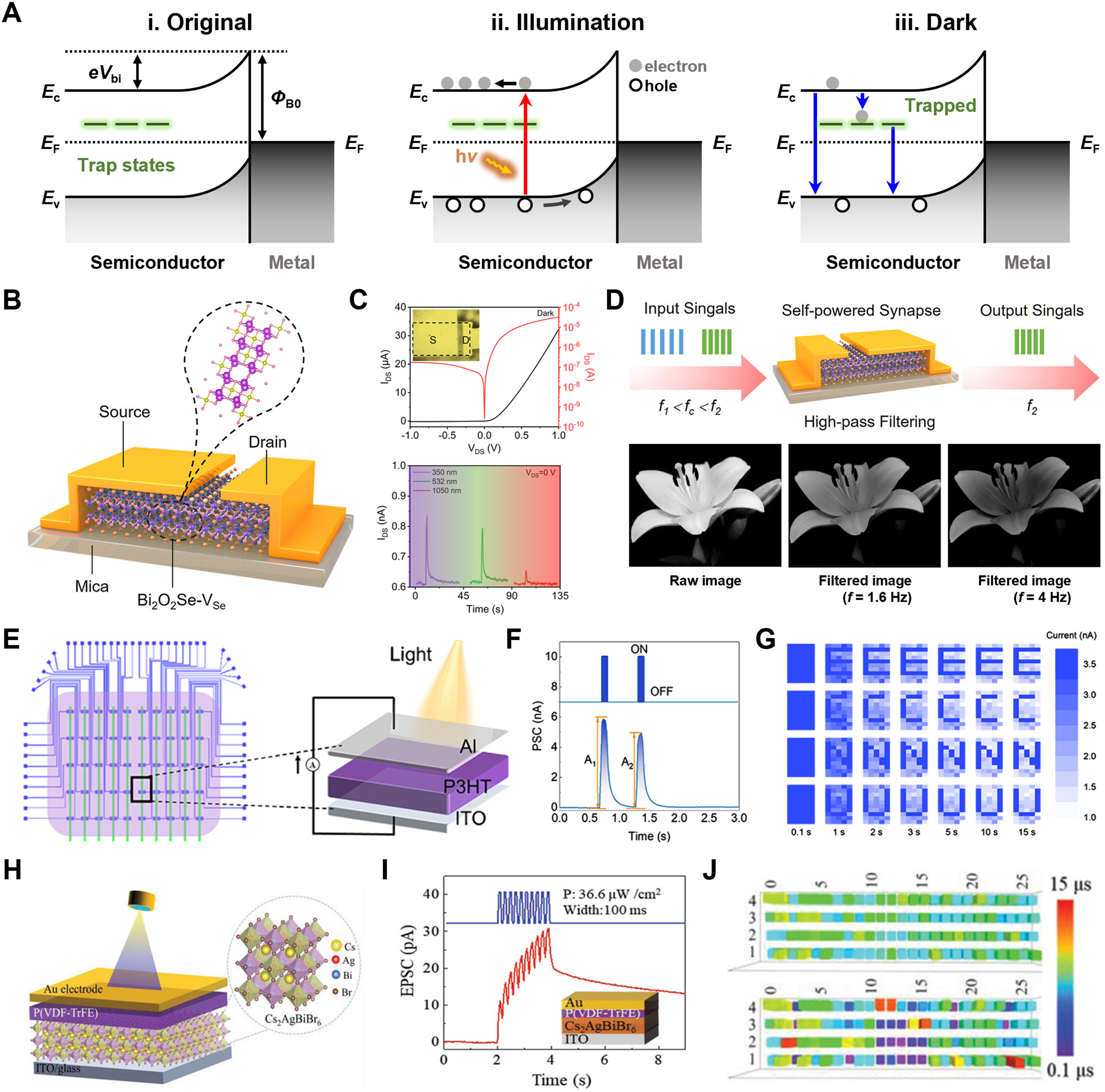
Figure 2. Schottky junction-based zero-power optoelectronic synapses. (A) Schematic illustrations of the working mechanism in a Schottky junction-based zero-power optoelectronic synapse correspond to the (i) original, (ii) illumination, and (iii) dark state, respectively. Ec, Ev and EF represent the bottom of conduction band, top of valence band, and Fermi level of the semiconductor, respectively. ΦB0, Vbi and e denote the work function of metal, built-in potential and elementary charge, respectively; (B) Schematic of the Bi2O2Se-VSe nanosheet-based zero-power optoelectronic synapse, with the inset highlighting the vacancy-rich atomic structure; (C) IDS depending on VDS characteristics of the device measured in dark conditions (top) and IDS without bias under illumination at wavelengths of 350, 532, and 1,050 nm (P = 66 μW·cm-2), demonstrating broadband photoreception (bottom); (D) Demonstration of high-pass filtering of the device. Subfigures (B-D) Reproduced with permission[32]. Copyright 2024, American Chemical Society; (E) Schematic illustration of a 10 × 5 array of ITO/P3HT/Al zero-power optoelectronic synapse; (F) Representative PSCs induced by two consecutive light pulses (λ = 520 nm, P = 215 mW·cm-2, duration = 100 ms, interval = 500 ms); (G) Photopic adaptation of the zero-power vision sensor array for pattern recognition. Subfigures (E-G) Reproduced with permission[33]. Copyright 2025, American Chemical Society; (H) Schematic illustration of the Cs2AgBiBr6-based zero-power photonic synapse; (I) Representative EPSC triggered by 10 light pulses (λ = 445 nm, P = 36.6 μW·cm-2) exhibiting in-sensor reservoir; (J) The weight modulation in the 25 × 4 array before and after the 50 training epochs for vehicle-flow classification. Subfigures (H-J) Reproduced with permission[34]. Copyright 2022, John Wiley & Sons. Bi2O2Se-VSe: Bi2O2Se nanosheet with selenium vacancies; ITO: indium tin oxide; P3HT: poly(3-hexylthiophene-2,5-diyl); PSCs: postsynaptic currents; EPSC: excitatory postsynaptic current; P(VDF-TrFE): poly(vinylidene fluoride-trifluoroethylene).
Ren et al. recently demonstrated a planar inorganic Schottky synapse based on single-crystalline Bi2O2Se nanosheets containing selenium vacancies (Bi2O2Se-VSe), synthesized via physical vapor deposition [Figure 2B][32]. The vacancy-induced trap states, together with the Schottky contact, enabled operation across a broad spectral range, from ultraviolet (UV) to near-infrared, without external electrical bias [Figure 2C]. The device exhibited typical synaptic characteristics, including EPSC, PPF, and STM-to-LTM transition, and further demonstrated frequency-dependent plasticity for high-pass optical filtering [Figure 2D].
To expand both spectral responsiveness and circuit-level adaptability, Dai et al. developed a zero-power retinomorphic photodiode array based on a Schottky junction between poly(3-hexylthiophene-2,5-diyl) (P3HT) and Al [Figure 2E][33]. The strong visible-light absorption of P3HT and defect-induced photogating allowed inhibitory postsynaptic current (IPSC) and paired-pulse depression (PPD), demonstrating reconfigurable learning behavior without external electrical bias [Figure 2F]. When integrated into a 10 × 5 array, the system successfully reproduced retina-inspired photopic adaptation, emulating the attenuation of signal intensity under prolonged illumination [Figure 2G].
To approach optical functionality of in-sensor reservoir computing, Lao et al. developed an ultralow-power machine vision system based on a zero-power sensor reservoir, exploiting a Schottky junction between the Cs2AgBiBr6 photosensitive layer and Au electrode [Figure 2H][34]. By embedding a ferroelectric-induced potential well at the shoulder of the Schottky barrier, the device significantly prolonged the dwell time of photogenerated carriers, thereby enabling nonlinear EPSC coupling under pulsed optical stimulation [Figure 2I]. This potential well-assisted carrier retention produces the spatiotemporally correlated EPSC responses essential for reservoir computing. The device exhibits key synaptic functions including PPF, spike-rate-dependent plasticity (SRDP) and spike-number-dependent plasticity (SNDP), demonstrating strongly tunable synaptic plasticity. In addition, the evolution of the 25 × 4 memristor conductance map from an initially random weight distribution to a well-trained configuration optimized for vehicle-flow classification [Figure 2J].
Heterojunction
Unlike Schottky junctions, heterojunctions form at the interface between two semiconductors with different band structures. Fermi-level alignment through charge transfer creates both conduction- and valence-band offsets, generating a built-in electric field that extends across the depletion region [Figure 3Ai][47,48]. Under illumination, excitons generated in the active layer dissociate only when they reach this interface, from which photogenerated electrons and holes are efficiently separated and driven in opposite directions, producing a photocurrent without external electrical bias [Figure 3Aii]. Concurrently, a portion of carriers becomes trapped at interfacial or defect-related states, and their gradual release after light removal induces persistent photocurrent relaxation, mimicking synaptic potentiation and depression under zero-power operation [Figure 3Aiii][37-42]. Compared with Schottky systems, heterojunctions offer more tunable band alignment and enhanced charge separation efficiency, enabling broader spectral sensitivity and more versatile synaptic behaviors. These characteristics make heterojunction-based zero-power optoelectronic synapses particularly attractive for zero-power operation, as synaptic modulation can be governed by interfacial band engineering. By carefully selecting semiconductor pairs with complementary energy levels, the built-in electric field and carrier transport pathways can be precisely controlled, modulating synaptic weight, retention time, and response speed. We review representative heterojunction-based optoelectronic synapses, highlighting operating principles, synaptic functionalities, and applications.

Figure 3. Heterojunction-based zero-power optoelectronic synapses. (A) Schematic illustrations of the working mechanism in heterojunction-based zero-power optoelectronic synapse correspond to the (i) original, (ii) illumination, and (iii) dark state, respectively. Ec, p, Ec, n, Ev, p, Ev, n, EF, p and EF, n represent the bottom of conduction band, top of valence band and Fermi levels of p-type and n-type semiconductors, respectively; (B) Schematic illustration of the vertically structured zero-power artificial photoreceptor based on the GaN/BiFeO3 heterojunction; (C) UV light-induced learning-forgetting-relearning behavior, demonstrating visual memory emulation in the GaN/BiFeO3-based neuromorphic sensor; (D) Visual memory emulation in a UV-sensitive artificial neuromorphic sensor. Subfigures (B-D) Reproduced with permission[37]. Copyright 2025, John Wiley & Sons; (E) Schematic illustration of the F16CuPc/C8-BTBT heterojunction-based zero-power artificial optoelectronic synapse; (F) SRDP triggered by ten consecutive light pulses, with a duration of 50 ms under different pulse frequencies; (G) Schematic illustration of an artificial visual system, in which the front-end signal processing units are integrated within the image sensor array. Subfigures (E-G) Reproduced with permission[38]. Copyright 2022, John Wiley & Sons; (H) Cross-sectional SEM image of the ZnO/WOX heterojunction-based zero-power optoelectronic memristor; (I) Photocurrent under constant light stimuli on a dark background; (J) Photocurrent response of the device under background illumination and flash stimulation, demonstrating Weber’s law behavior; (K) Schematic diagram of the neuromorphic visual system, consisting of adaptive image preprocessing using a visual adaptive neuron and image recognition using a spiking neural network; (L) Spontaneous adaptation of overexposed images based on the experimentally observed frequency-dependent relaxation dynamics of the visual adaptive neuron. Subfigures (H-L) Reproduced with permission[39]. Copyright 2025, John Wiley & Sons. UV: Ultraviolet; C8-BTBT: dioctylbenzothienobenzothiophene; SRDP: spike-rate-dependent plasticity; EPSC: excitatory postsynaptic current; PMMA: poly(methyl methacrylate); ITO: indium tin oxide.
Zheng et al. reported a retina-inspired optoelectronic synapse based on a vertical GaN/BiFeO3 heterojunction [Figure 3B][37]. The ferroelectric BiFeO3 layer, containing abundant oxygen vacancies, acted as both a UV absorber and a charge-trapping reservoir. The built-in photovoltaic field across the heterojunction enabled operation without external electrical bias under ultra-weak UV illumination. The device exhibited a wide range of synaptic plasticity, including EPSC, PPF, STM-to-LTM transition, and learning-forgetting-relearning behavior, with a maximum PPF index of 200% and a minimum detectable UV intensity of 0.68 μW·cm-2 [Figure 3C]. UV-modulated negative polarization and vacancy ionization enhanced persistent photoconductivity, allowing the synaptic weight to be modulated by invisible UV light and used for pattern recognition, including letter images [Figure 3D].
Beyond inorganic systems, Hao et al. developed zero-power artificial optoelectronic synapses based on ultrathin organic asymmetric C8-BTBT (dioctylbenzothienobenzothiophene)/F16CuPc (copper hexadecafluorophthalocyanine) heterojunction films [Figure 3E][38]. The efficient conversion of UV light into photocurrent enabled zero-bias synaptic functions such as EPSC, PPF, and SRDP without external electrical bias. Specifically, the SRDP behavior allows high-pass filtering for image preprocessing with a cutoff frequency of 6.9 Hz [Figure 3F]. This high-pass filtering effect was further utilized for image sharpening, where slowly varying background components were suppressed while high-frequency edge features were selectively enhanced, enabling more efficient visual recognition [Figure 3G]. By tuning gate voltage to modulate interfacial charge transfer, the platform extended its response from UV to the near-infrared region, achieving multispectral sensing and expanding the perceptual range beyond that of the biological retina.
Cheng et al. demonstrated a zero-power optoelectronic memristor based on a ZnO/WOX heterojunction [Figure 3H], capable of mimicking key retinal adaptation phenomena, including desensitization and Weber’s law[39]. Under pulsed optical stimulation without an external electrical bias, the photovoltaic effect, coupled with charge trapping at the heterojunction, produced transient postsynaptic currents with gradual decay, analogous to photoreceptor adaptation [Figure 3I]. The device further exhibited background-dependent response to flash stimuli, representing Weber’s law [Figure 3J]. By integrating the memristor with a NbOX-based threshold-switching element, the system converted continuous light inputs into dynamic spike trains, enabling adaptive image preprocessing and overexposed image recognition with high accuracy [Figure 3K and L].
PTE effect
The PTE effect converts absorbed light into a temperature gradient, generating a Seebeck voltage and thermally driven photocurrent for zero-bias operation with bandgap-independent spectral response[49]. Although the thermally driven response is slower than photovoltaic detectors, such intrinsic temporal delays are beneficial for emulating biological synaptic plasticity, particularly gradual potentiation and relaxation. Recently, this concept has been extended from conventional electron-driven Seebeck systems to ion-conductive materials, utilizing heterostructures engineered with distinct photothermal properties and Seebeck coefficients [Figure 4Ai][43-45]. Unlike Schottky or heterojunction systems that rely primarily on electronic carrier trapping, light-induced thermal gradients drive asymmetric ion migration, establishing directional ionic transport that modulates photoconductance without external electrical bias [Figure 4Aii]. Following illumination, slow thermal relaxation, progressive ion redistribution, and defect-assisted thermoelectric modulation induce persistent conductance changes analogous to long-term synaptic behavior [Figure 4Aiii]. The zero-power optoelectronic synapses based on PTE effect using ionogel heterostructure offer inherent mechanical softness, flexibility, and stretchability. Thus, the PTE effect-based zero-power optoelectronic synapses exhibit stable synaptic functionality under bending, stretching, and repeated mechanical deformation, highlighting their robustness for soft and body-interfaced applications compared to Schottky junction- and heterojunction-based synapses. The soft PTE-effect-based zero-power optoelectronic synapses are particularly promising candidates for wearable neuromorphic platforms.
Figure 4. PTE-based zero-power optoelectronic synapses. (A) Schematic illustrations of the working mechanism in PTE-based zero-power optoelectronic synapse correspond to the (i) original, (ii) illumination, and (iii) dark state, respectively. Danion and Dcation represent the anion and cation diffusion coefficient, respectively; (B) Schematic illustration of artificial neuromorphic vision skin based on a silver nanoparticle-doped ionogel heterostructure; (C) Optical synaptic characteristics of the devices in the planar state and under different curvatures; (D) Optical images of the flexible neuromorphic vision skin device attached to human skin. Subfigures (B-D) Reproduced with permission[43]. Copyright 2025, IOP Publishing; (E) Schematic illustration of the zero-power ionogel photoreceptor; (F) Photoresponse of the device under 365 nm illumination without an external power; (G) PPF index as a function of light stimulus interval; (H) Optical images of photoreceptor transplantation by replacing a damaged pixel with a healthy one in the host retina; (I) Visual restoration in the “I” mapping after photoreceptor transplantation; (J) Optical images and schematic illustration of the real-time motion tracking testing measurement setup; (K) Schematic of the laser spot motion path and real-time trajectory tracking at different speeds, demonstrating motion direction and perception capability. Subfigures (E-K) Reproduced with permission[44]. Copyright 2024, Springer Nature. PTE: Photothermoelectric; HBA: 4-hydroxybutyl acrylate; EOEOEA: 2-(2-ethoxyethoxy)ethyl acrylate; TFSI-: bis(trifluoromethanesulfonyl)imide anion; AgNPs: silver nanoparticles; PPy-NP: polypyrrole nanoparticle; PPF: paired-pulse facilitation; EPSC: excitatory postsynaptic current; SHR-E: self-powered hemispherical retinomorphic eye; TIA: trans-impedance amplifier; DAQ: data acquisition.
Qian et al. reported an artificial neuromorphic vision skin based on a silver nanoparticle-doped ionogel heterostructure exhibiting zero-power operation, self-healing, mechanical flexibility, and photonic synaptic processing [Figure 4B][43]. Localized surface plasmon resonance in the embedded nanoparticles converted light into heat, establishing a temperature gradient that drove directional ion migration through the PTE mechanism. The ion flux produced photosynaptic behaviors such as EPSC, PPF, and gradually accumulated responses under repeated illumination, while reversible hydrogen bonds within the polymer network provided mechanical resilience [Figure 4C]. When assembled into a 5 × 5 photosynaptic array, the ionogel skin sensed, memorized, and reconstructed light patterns on both flat and curved surfaces, functioning as a conformal neuromorphic imager [Figure 4D].
Luo et al. realized a bionic hemispherical retinomorphic eye, in which an elastomeric retina composed of an ionogel heterojunction pillar array acted as photosynaptic photoreceptors [Figure 4E][44]. Driven by the PTE effect, doped and undoped ionogel regions generated temperature differences under broadband illumination (365 to 970 nm), inducing asymmetric Li+/bis(trifluoromethanesulfonyl)imide anion (TFSI-) migration and a built-in potential that produced neuroelectric signals with pronounced synaptic plasticity without external electrical bias [Figure 4F and G]. The soft ionogel retina conformally laminated onto arbitrary curved surfaces and was further assembled into a 5 × 5 transplantable photosynaptic patch to restore photocurrent in defective regions, mimicking retinal repair [Figure 4H and I]. The integrated system exhibited neuromorphic image learning, forgetting, and real-time motion tracking using spatiotemporal voltage mapping [Figure 4J and K].
CHALLENGES
Despite the rapid progress in zero-power optoelectronic synapses, several scientific and engineering challenges remain before these technologies can evolve into practical wearable neuromorphic systems. These limitations stem not only from the intrinsic constraints of materials and device architectures but also from the requirements unique to zero-power, body-interfaced systems, such as operation under low-intensity illumination, mechanical deformation, and spatiotemporally varying environments. The realization of energy-autonomous, mechanically compliant, and long-term stable systems requires advances across multiple dimensions, ranging from light-matter interactions and synaptic plasticity to structural design and large-area integration with mechanical softness. In this section, we discuss five key challenges [Figure 5], including limited light utilization, insufficient adaptive learning capability, environmental instability, lack of system-level integration, and mechanical incompatibility.
Figure 5. Challenges for zero-power optoelectronic synapses in future wearable neuromorphic systems.
Moreover, we provide a forward-looking perspective on how these challenges may be addressed by drawing on insights from prior advances in optoelectronics, wearable electronics, and soft material systems [Figure 6]. Rather than focusing on isolated device improvements, we outline possible technological directions for overcoming key limitations, thereby offering a roadmap toward practical and scalable zero-power neuromorphic wearable platforms. In the following sections, detailed strategies are discussed for each challenge, highlighting how coordinated progress in materials design, device physics, and system-level architecture could collectively enable practical, scalable, and truly zero-power neuromorphic wearable platforms.
Figure 6. Future outlook for zero-power optoelectronic synapses for wearable neuromorphic platforms. Reproduced with permission[50]. Copyright 2025, American Chemical Society. Reproduced with permission[51]. Copyright 2024, John Wiley & Sons. Reproduced with permission[52]. Copyright 2021, Springer Nature. Reproduced with permission[53]. Copyright 2024, American Chemical Society. Reproduced with permission[54]. Copyright 2021, John Wiley & Sons. Reproduced with permission[55]. Copyright 2022, IOP Publishing. Reproduced with permission[56]. Copyright 2020, American Chemical Society. Reproduced with permission[57]. Copyright 2025, John Wiley & Sons. Reproduced with permission[58]. Copyright 2021, Springer Nature. Reproduced with permission[59]. Copyright 2019, American Chemical Society. Reproduced with permission[60]. Copyright 2023, John Wiley & Sons. Reproduced with permission[61]. Copyright 2015, John Wiley & Sons. Reproduced with permission[62]. Copyright 2018, John Wiley & Sons. BHJ: Bulk heterojunction; CTE: charge-transfer emission; OLED: organic light-emitting diode; OPV: organic photovoltaic; PSC: postsynaptic current; ETL: electron transport layer; HTL: hole transport layer; EPSC: excitatory postsynaptic current; IPSC: inhibitory postsynaptic current; ITO: indium tin oxide; IGZO: indium gallium zinc oxide; ST: synaptic transistor; TSM: threshold switching memristor; GND: ground.
Limited light utilization
The performance of zero-power optoelectronic synapses is determined by not only how efficiently light is absorbed and converted into electrical or photothermal signals, but also how effectively these light-induced processes modulate and retain synaptic weights. In zero-power systems, where no external electrical bias is available to assist charge separation or amplification, achieving sufficient photoresponsivity becomes even more critical for sensing-in-memory operation[63]. A higher responsivity further expands the dynamic range of photocurrent and enables finer control over the synaptic weights, thereby increasing the number of accessible conductance states and improving the precision of learning[64,65]. Conversely, insufficient responsivity restricts synaptic modulation to a narrow multi-level synaptic weight, leading to coarse weight updates and degraded learning accuracy. This limitation is particularly detrimental for neuromorphic systems that require gradual and analog weight tuning to emulate biological learning processes. However, in most current devices, the internal driving forces generated by built-in potentials or thermal gradients are relatively weak, resulting in low photocurrent and limited weight modulation[42,66]. Consequently, strong illumination is often required to trigger learning behavior, which contradicts the zero-power concept and limits applicability under ambient lighting or typical visual perception conditions. Therefore, enhancing light-matter coupling and exciton dissociation efficiency under low-intensity illumination will be crucial to realizing practical zero-power operation in wearable environments.
Future strategies should focus on improving photon management within soft and deformable platforms. Incorporating microstructured surfaces, photonic crystal layers, or plasmonic nanostructures can enhance light scattering and confinement without compromising mechanical flexibility[67,68]. In addition, hybridization with high-absorption nanomaterials such as quantum dots (QDs) or perovskite nanoparticles could broaden the spectral response, enabling more efficient energy harvesting from broadband illumination[69,70]. The photoactive components with inherently high absorption coefficients and strong light-matter interactions are an effective strategy for enhancing photon harvesting, particularly under low-intensity illumination. Specifically, QDs offer size-tunable bandgaps that allow the absorption spectrum to be precisely engineered, enabling enhanced light efficiency at user-selective wavelengths. In parallel, device structure engineering plays a crucial role in enhancing light utilization efficiency by increasing the effective optical interaction length and facilitating efficient carrier separation. In particular, the shortened channel length of a vertical architecture can facilitate efficient charge separation, enabling higher light utilization under weak illumination. Adapting these material and structural designs to zero-power optoelectronic synapses may enable a stronger photoresponse and more efficient synaptic modulation under low light intensity, thereby improving device performance under realistic wearable operating conditions. Therefore, beyond conventional responsivity enhancement, future approaches must focus on maximizing light-matter interaction under low-intensity and broadband illumination while remaining compatible with soft, deformable platforms.
Insufficient adaptive learning capability
Most reported zero-power optoelectronic synapses primarily exhibit unidirectional weight modulation, typically light-induced potentiation followed by passive relaxation. This behavior originates from the limited capability to reversibly control carrier trapping and detrapping under zero-bias conditions, leading to gradual saturation of the synaptic state and a loss of learning flexibility[32-39,41-45,66]. For neuromorphic operation, however, devices must achieve hardware-level adaptive learning through both potentiation and depression to dynamically adjust synaptic weights in response to varying optical stimuli. In addition, on-demand resetting, facilitated by bidirectional weight modulation, is essential to restore baseline states and prevent weight accumulation. This bidirectional modulation is particularly important in zero-power systems, where no external electrical resetting is available, and synaptic states must be optically reconfigurable without energy-consuming processes. In artificial neural networks, bidirectional weight modulation is fundamentally required to enable stable, efficient, and adaptive learning[71-73]. Neuromorphic learning relies on the coordinated strengthening and weakening of synaptic weight updates across multiple layers. When synaptic updates occur only through potentiation, synaptic weights tend to increase excessively, leading to overfitting and imposing fundamental limitations on learning stability, adaptability, and generalization in artificial neural networks. Once saturation is reached, further learning becomes ineffective because synapses lose the dynamic range required to encode new information. These limitations severely hinder learning accuracy, error correction, and feedback. Therefore, bidirectional weight modulation is not merely a desirable device characteristic but also a prerequisite for neuromorphic networks.
Achieving bidirectional modulation under zero-power operation requires new approaches that enable controlled depression without external electrical bias. While conventional optoelectronic synapses in transistor configurations typically rely on electrical gating to induce depression[74,75], such methods undermine the zero-power concept. Alternative strategies, such as using different optical wavelengths or spatially patterned illumination demonstrated in bias-dependent devices[76-78], may provide optical routes for bidirectional weight control while maintaining energy autonomy. To achieve bidirectional weight modulation, heterojunction-based optoelectronic synapses indicate wavelength-selective photoexcitation pathways through distinct optical absorption spectra, energy bandgaps, and energy band alignments[40,79-81]. The different optical properties of heterojunction semiconductors enable selective generation of dominant charge carrier in one semiconductor layer, depending on the incident light wavelength. This wavelength-dependent carrier selectivity directly enables bidirectional weight modulation by controlling the transport of photogenerated carriers. Extending this design principle to zero-power optoelectronic synapses suggests a practical pathway toward stable bidirectional learning without external electrical bias. The consideration of the optical properties of semiconductor pairs and careful engineering of heterojunction interfaces, wavelength-selective absorption can be directly translated into controlled carrier dynamics, thereby improving the precision and repeatability of synaptic weight updates.
Additionally, conventional neuromorphic computing primarily relies on electrically driven conductance modulation for learning[82-84]. However, in zero-power optoelectronic synapses, the absence of external electrical bias precludes conductance-based neuromorphic computing. Thus, the development of new learning paradigms and system architectures for zero-power optoelectronic synapses is essential. Although these approaches remain in their early stages, exploring such optical pathways will be essential for realizing fully adaptive and energy-efficient zero-power neuromorphic devices.
Instability and variability
Ensuring reliable and consistent operation remains one of the most critical challenges for zero-power optoelectronic synapses. Under repeated optical stimulation or prolonged environmental exposure, devices often exhibit drift in conductance states, inconsistent cycle-to-cycle responses, and noticeable device-to-device variation[85,86]. In realistic wearable environments, zero-power optoelectronic synapses must operate reliably under continuous exposure to moisture, sweat, and UV light in daily human life. Ensuring stable device performance under sweat and high-humidity conditions requires encapsulation to protect the device from moisture, hydrated complexes inducing irreversible performance degradation. In addition, photonic safety and feasibility under continuous exposure, especially UV light, must be carefully considered to ensure long-term operational stability in wearable applications.
This instability not only undermines reproducibility at the individual device level but also becomes increasingly problematic when multiple synapses are integrated into array networks, where cumulative variability can severely degrade overall system performance. Unlike conventional electrically driven synapses, where active biasing can assist stabilization, zero-power synapses rely solely on passive photonic or ionic mechanisms. This makes them more susceptible to instability caused by trap dynamics, environmental fluctuations, and mechanical perturbations. Minor differences in material composition, processing history, or interface quality can therefore translate into large disparities in the synaptic response, even among nominally identical devices. Such sensitivity to subtle variations poses a serious challenge for large-area fabrication and scaling, where maintaining precise control over material uniformity and interfacial quality is inherently difficult. In wearable environments, this challenge is further exacerbated by continuously changing temperature, humidity, and mechanical strain. As a result, instability and variability represent not only device-level concerns but also system-level obstacles that fundamentally limit the reliability, scalability, and long-term stability of zero-power optoelectronic synapses in practical wearable neuromorphic platforms.
Future development should prioritize stability throughout the entire device configuration from active materials to interfacial contact. Robust material systems with intrinsic chemical and thermal stability, as well as self-regulated trap-state dynamics under environmental and temporal fluctuations, are required to sustain consistent performance over time[54,87,88]. In parallel, encapsulation technologies must advance beyond conventional protective layers to provide not only high environmental resistance but also mechanical compliance and optical transparency. Moreover, suppressing device-to-device variability is essential for ensuring reproducible synaptic behavior, particularly when zero-power optoelectronic synapses are integrated into large-scale arrays. The device variability induced by film thickness, interfacial quality, defect density, and local trap distributions can lead to substantial differences in photoresponse, conductance modulation range, and temporal plasticity[89-91]. To reduce variability, fabrication strategies that ensure uniformity, morphology, and consistent material properties are required. In addition, adopting chemical vapor deposition for thin-film deposition techniques may further reduce the variability of zero-power optoelectronic synapses[92,93]. Establishing such advanced reliability will be crucial for realizing zero-power optoelectronic synapses that exhibit stable, predictable performance in wearable neuromorphic platforms operating under dynamic, body-interfaced environments.
Lack of system-level integration
Although individual zero-power optoelectronic synapses have demonstrated promising performance, their translation into functional large-scale systems remains highly limited. While promising synaptic behaviors have been demonstrated at the device level, zero-power architectures impose additional constraints at the system level, particularly in terms of synchronization, crosstalk suppression, and reliable optical communication without external driving circuitry[36,41,42]. Thus, reproducible computation and reliable signal transfer across networks are not yet achievable. The absence of circuit-level investigations further impedes progress toward practical neuromorphic applications, such as hardware-based image recognition or vector-matrix multiplication, where coordinated and uniform device behavior is essential for accurate parallel processing.
To bridge the gap, system-level integration must be achieved through concurrent optimization of materials, device architecture, fabrication strategies, and circuit design. In parallel, scalable manufacturing methods such as printing, transfer assembly, or hybrid stacking can facilitate realistic integration of soft and deformable systems. These approaches allow large-area fabrication while preserving material softness and structural integrity. At the circuit level, implementing passive optical interconnects or wavelength-selective channels may help minimize crosstalk and reduce power demand during complex data processing. Optical waveguides allow optical signals to be distributed across synaptic arrays, reducing optical crosstalk and improving addressability at the system level with low-leakage electrical readout[56,94]. The system-level circuit should be carefully designed with respect to optical routing and electrical readout to ensure that signal extraction incurs no electrical overhead from peripheral readout, amplification, or signal circuitry. Ultimately, achieving uniformity and stability across dense arrays will be key to transforming zero-power optoelectronic synapses from proof-of-concept devices into fully functional neuromorphic systems for wearable applications.
Mechanical incompatibility
For practical wearable systems, devices must maintain stable performance under continuous and multidirectional mechanical deformation while preventing functional failure, physical damage, and user discomfort to ensure long-term reliability and safety during skin contact. To verify the feasibility of wearable platforms, mechanical reliability experiments are essential. Beyond simple bending tests, devices must be evaluated under cyclic tensile and compressive strain experiments to ensure long-term wearable stability. Moreover, optoelectronic synaptic characterization during deformation is required to directly correlate mechanical strain with changes in synaptic weight modulation, retention, and variability. The mechanical reliability is indispensable for validating the practical applicability of zero-power optoelectronic synapses in wearable neuromorphic platforms. However, most reported zero-power optoelectronic synapses remain mechanically fragile, relying on rigid or semi-flexible substrates that cannot tolerate realistic deformation[35-42]. Mechanical degradation phenomena such as cracking, delamination, or the formation of microdefects further induce irreversible resistance changes, exacerbating functional instability. In addition, the mechanical mismatch between rigid device components and the soft human body causes discomfort and limits conformal contact, hindering seamless integration and high-fidelity biosignal monitoring. Although certain PTE-based systems employing ionogel or elastomeric substrates have demonstrated inherent softness, softness alone does not guarantee stable synaptic function under strain. In zero-power configurations relying on built-in or thermoelectric fields, even minor interfacial distortions can disrupt charge or ion transport pathways, resulting in degraded or unpredictable synaptic weight modulation. Furthermore, PTE-based devices inherently rely on localized heating, which affects other electronic components in integrated circuits and induces thermal crosstalk between neighboring synapses. Thus, PTE-based devices require careful thermal isolation and architectural design to ensure reliable operation in wearable neuromorphic platforms.
These limitations can be addressed by adopting design principles from soft electronics and by developing new material systems specifically optimized for zero-power operation. The mechanical softness of all device components including the substrate, electrodes, active layer, and encapsulation layer must be carefully considered to ensure compatible mechanical properties. Mechanical mismatch among all components can lead to stress concentration, interfacial delamination, and irreversible performance degradation under mechanical deformation. For the substrate and encapsulation layers, hydrophobic elastomeric materials with intrinsic softness and optical transparency can be employed to provide mechanical compliance while maintaining synaptic performances and preventing environmental defects[95-97]. Soft electrodes can be achieved by embedding nanoscale conductive materials in polymer matrices or by using crosslinking additives to improve flexibility while maintaining electrical conductivity[58,98,99]. The development of intrinsically stretchable semiconductors and the formation of semiconductor composites with elastomeric materials are strategies for providing softness to active layer[100,101]. In particular, advancing intrinsically stretchable electronic materials can enhance mechanical robustness without complex fabrication processes[102-104]. However, such approaches must also preserve the delicate trap-state dynamics that govern synaptic behavior, as local trap distributions and carrier pathways are easily perturbed by mechanical strain, even subtle interfacial distortions can result in signal drift or performance degradation. Moreover, reducing film thickness enhances stretchability by lowering bending stiffness and surface strain, allowing mechanical deformation to be accommodated elastically rather than through fracture or delamination. Translating such material and structural design principles to zero-power optoelectronic synapses is expected to help maintain stable optoelectronic functionality under mechanical deformation, which is applicable in wearable platforms.
In this context, extending all-soft structural engineering to Schottky junction and heterojunction-based zero-power optoelectronic synapses offers a promising pathway to construct mechanical stability for wearable neuromorphic platforms. Therefore, next-generation designs should aim to minimize perturbations in synaptic weight states to ensure reliable learning and processing under deformation induced by conformal body motion. Achieving this goal represents a distinct challenge compared with conventional stretchable devices, requiring materials and architectures that sustain both elasticity and neuromorphic fidelity under dynamic deformation.
CONCLUSION AND OUTLOOK
Zero-power optoelectronic synapses mark a key inflection point in the evolution of neuromorphic electronics, providing a foundation for devices that perceive, learn, and adapt using light as their sole energy source to minimize power consumption during system operation. Recent advances have demonstrated that built-in potential and PTE effect can drive synaptic functions without external electrical bias, highlighting the potential for unprecedented energy efficiency. However, realizing fully autonomous, deformable, and intelligent systems requires overcoming multiple challenges, including photon management, bidirectional learning, operational stability, mechanical adaptability, and scalable system-level integration.
Addressing these challenges demands cross-disciplinary efforts that connect materials chemistry, device physics, and circuit and architectural design, rather than focusing on isolated device improvements. To address limited light utilization, future research should focus on enhancing light-matter interactions through advanced photon-management strategies, including high absorption photoactive materials and vertical structure. Insufficient adaptive learning capability may be overcome by designing wavelength-selective optoelectronic synapses, particularly through heterojunction engineering that enables controllable bidirectional charge carrier transport and reversible weight modulation without external electrical bias. Device instability and variability can be addressed by an encapsulation process using hydrophobic transparent materials to prevent environmental defects and by achieving a precise and uniform film morphology. Achieving system-level integration requires extending device-level advances toward array-based architectures, incorporating optical waveguides, passive optical interconnects, and wavelength-division to suppress crosstalk and enable scalable in-sensor computing. Developing intrinsically soft electronic materials and mechanically reliable interfaces will be as crucial as designing architectures that preserve neuromorphic fidelity under dynamically changing environmental and physiological conditions. Furthermore, integrating optical interconnects and scalable fabrication strategies will be essential for translating device-level concepts into practical systems capable of hardware-based image recognition and vector-matrix computation.
In the end, the convergence of zero-power operation, mechanical compliance, and neuromorphic intelligence will define the next phase of wearable technology. Future systems are expected to evolve beyond discrete sensing modules into fully integrated, adaptive networks capable of continuous perception, energy regulation, and physiological interpretation within body-interfaced environments. By autonomously managing energy flow and decoding multimodal biosignals, these platforms could function as intelligent companions for long-term health monitoring and responsive therapeutic control. Ultimately, this shift toward zero-power, soft, and cognitively capable electronics will not only advance wearable systems but also redefine how human-machine interfaces enable sustainable and lifelong interaction with the body, environment, and technology.
DECLARATIONS
Authors’ contributions
Conceived the topic: Na, M.; Park, J.; Sim, K.
Original draft writing: Na, M.; Park, J.; Sim, K.
Supervised and reviewed the manuscript: Sim, K.
Availability of data and materials
Not applicable.
AI and AI-assisted tools statement
During the preparation of this manuscript, the AI-based tool Springer Nature's Curie was used solely for language editing. The tool did not influence the study design, data collection, analysis, interpretation, or the scientific content of the work. All authors take full responsibility for the accuracy, integrity, and final content of the manuscript.
Financial support and sponsorship
This work was supported by the National Research Foundation of Korea (NRF) grant funded by the Korean government, Ministry of Science and ICT (No. RS-2024-00346943).
Conflicts of interest
All authors declared that there are no conflicts of interest.
Ethical approval and consent to participate
Not applicable.
Consent for publication
Not applicable.
Copyright
© The Author(s) 2026.
REFERENCES
1. Jang, H.; Lee, J.; Beak, C. J.; Biswas, S.; Lee, S. H.; Kim, H. Flexible neuromorphic electronics for wearable near-sensor and in-sensor computing systems. Adv. Mater. 2025, 37, e2416073.
2. Shi, Q.; Dong, B.; He, T.; et al. Progress in wearable electronics/photonics—moving toward the era of artificial intelligence and internet of things. InfoMat 2020, 2, 1131-62.
3. Kim, S. H.; Baek, G. W.; Yoon, J.; et al. A bioinspired stretchable sensory-neuromorphic system. Adv. Mater. 2021, 33, e2104690.
4. Linh, V. T. N.; Han, S.; Koh, E.; Kim, S.; Jung, H. S.; Koo, J. Advances in wearable electronics for monitoring human organs: bridging external and internal health assessments. Biomaterials 2025, 314, 122865.
5. Gu, Y.; Zhang, T.; Chen, H.; et al. Mini review on flexible and wearable electronics for monitoring human health information. Nanoscale. Res. Lett. 2019, 14, 263.
6. Kim, H.; Kim, D.; Kim, J.; et al. Advances and perspectives in fiber-based electronic devices for next-generation soft systems. npj. Flex. Electron. 2025, 9, 84.
7. Pan, S.; Wu, S.; Ming, J.; Ling, H. Toward energy-efficient machine vision: advances in optoelectronic memristors. Adv. Opt. Mater. 2025, 13, e01992.
8. Yao, P.; Wu, H.; Gao, B.; et al. Fully hardware-implemented memristor convolutional neural network. Nature 2020, 577, 641-6.
9. Schuman, C. D.; Kulkarni, S. R.; Parsa, M.; Mitchell, J. P.; Date, P.; Kay, B. Opportunities for neuromorphic computing algorithms and applications. Nat. Comput. Sci. 2022, 2, 10-9.
10. Shim, H.; Sim, K.; Ershad, F.; et al. Stretchable elastic synaptic transistors for neurologically integrated soft engineering systems. Sci. Adv. 2019, 5, eaax4961.
11. Upadhyay, N. K.; Jiang, H.; Wang, Z.; Asapu, S.; Xia, Q.; Joshua Yang, J. Emerging memory devices for neuromorphic computing. Adv. Mater. Technol. 2019, 4, 1800589.
12. Lee, J. W.; Han, J.; Kang, B.; Hong, Y. J.; Lee, S.; Jeon, I. Strategic development of memristors for neuromorphic systems: low-power and reconfigurable operation. Adv. Mater. 2025, 37, 2413916.
13. Zhang, J.; Dai, S.; Zhao, Y.; Zhang, J.; Huang, J. Recent progress in photonic synapses for neuromorphic systems. Adv. Intell. Syst. 2020, 2, 1900136.
14. Chen, X.; Chen, B.; Jiang, B.; et al. Nanowires for UV-vis-IR optoelectronic synaptic devices. Adv. Funct. Mater. 2023, 33, 2208807.
15. Sun, Y.; Ding, Y.; Xie, D. Mixed-dimensional van der Waals heterostructures enabled optoelectronic synaptic devices for neuromorphic applications. Adv. Funct. Mater. 2021, 31, 2105625.
16. Lee, J.; Jeong, B. H.; Kamaraj, E.; et al. Light-enhanced molecular polarity enabling multispectral color-cognitive memristor for neuromorphic visual system. Nat. Commun. 2023, 14, 5775.
17. Jiang, T.; Wang, Y.; Huang, W.; et al. Retina-inspired organic neuromorphic vision sensor with polarity modulation for decoding light information. Light. Sci. Appl. 2023, 12, 264.
18. Ahmed, T.; Tahir, M.; Low, M. X.; et al. Fully light-controlled memory and neuromorphic computation in layered black phosphorus. Adv. Mater. 2021, 33, 2004207.
19. Jiang, T.; Wang, Y.; Zheng, Y.; et al. Tetrachromatic vision-inspired neuromorphic sensors with ultraweak ultraviolet detection. Nat. Commun. 2023, 14, 2281.
20. Ren, Q.; Zhu, C.; Ma, S.; et al. Optoelectronic devices for in-sensor computing. Adv. Mater. 2025, 37, 2407476.
21. Wang, J.; Ilyas, N.; Ren, Y.; et al. Technology and integration roadmap for optoelectronic memristor. Adv. Mater. 2024, 36, 2307393.
22. Shim, S.; Kim, S.; Lee, D.; et al. Infrared-triggered retinomorphic artificial synapse electronic device containing multi-dimensional van der Waals heterojunctions. Small 2025, 21, 2410892.
23. Park, H.; Kim, D.; Kim, S.; Na, M.; Kim, Y.; Sim, K. Chemically and physically enhanced adhesion for robust interfaces in all-soft vertical organic photodetectors. Chem. Commun. 2024, 60, 9262-5.
24. Lan, L.; Huang, B.; Li, Y.; et al. Stretchable optoelectronic synapses with ultraviolet to near-infrared perception for retina-inspired computing and vision-adaptive sensing. npj. Flex. Electron. 2025, 9, 16.
25. Zhang, J.; Sun, T.; Zeng, S.; et al. Tailoring neuroplasticity in flexible perovskite QDs-based optoelectronic synaptic transistors by dual modes modulation. Nano. Energy. 2022, 95, 106987.
26. Kim, K. N.; Sung, M. J.; Park, H. L.; Lee, T. W. Organic synaptic transistors for bio-hybrid neuromorphic electronics. Adv. Electron. Mater. 2022, 8, 2100935.
27. Chang, K. C.; Liu, H.; Duan, X.; Peng, Z.; Lin, X.; Li, L. Optoelectronic dual-synapse based on wafer-level GaN-on-Si device incorporating embedded SiO2 barrier layers. Nano. Energy. 2024, 125, 109564.
28. Yin, L.; Huang, W.; Xiao, R.; et al. Optically stimulated synaptic devices based on the hybrid structure of silicon nanomembrane and perovskite. Nano. Lett. 2020, 20, 3378-87.
29. Wang, H.; Jiang, S.; Hao, Z.; et al. Molecular-layer-defined asymmetric Schottky contacts in organic planar diodes for self-powered optoelectronic synapses. J. Phys. Chem. Lett. 2022, 13, 2338-47.
30. Huang, W.; Hang, P.; Xia, X.; et al. Two-terminal self-rectifying optoelectronic synaptic devices with largest-dynamic-range updates. Appl. Mater. Today. 2023, 30, 101728.
31. Wang, K.; Wu, J.; Wang, M.; et al. A biodegradable, stretchable, healable, and self-powered optoelectronic synapse based on ionic gelatins for neuromorphic vision system. Small 2024, 20, 2404566.
32. Ren, X.; He, X.; Duan, Z.; et al. Self-powered and broadband optical synapse device based on Se-vacancy Bi2O2Se for artificial vision system application. ACS. Photonics. 2024, 11, 4990-9.
33. Dai, Y.; Hao, S.; Feng, G.; et al. A self-powered organic vision sensor array for photopic adaptation. Nano. Lett. 2025, 25, 2878-86.
34. Lao, J.; Yan, M.; Tian, B.; et al. Ultralow-power machine vision with self-powered sensor reservoir. Adv. Sci. 2022, 9, 2106092.
35. Yang, C.; Su, L.; Xia, K.; Li, X.; Liu, Y.; Li, H. Doping-modulated lateral asymmetric Schottky diode as a high-performance self-powered synaptic device. Opt. Express. 2023, 31, 31061-71.
36. Zhao, P.; Cui, M.; Li, Y.; et al. Self-powered optoelectronic artificial synapses based on a lead-free perovskite film for artificial visual perception systems. J. Mater. Chem. C. 2023, 11, 6212-9.
37. Zheng, X.; Dong, M.; Li, Q.; et al. Retina-inspired artificial synapses with UV modulated and immediate switchable plasticity. Adv. Funct. Mater. 2025, 35, 2420612.
38. Hao, Z.; Wang, H.; Jiang, S.; et al. Retina-inspired self-powered artificial optoelectronic synapses with selective detection in organic asymmetric heterojunctions. Adv. Sci. 2022, 9, 2103494.
39. Cheng, Y.; Zhang, J.; Lin, Y.; et al. Bioinspired adaptive neuron enabled by self-powered optoelectronic memristor and threshold switching memory for neuromorphic visual system. Adv. Sci. 2025, 12, 2417461.
40. Lao, J.; Jiang, C.; Luo, C.; et al. Self-powered and humidity-modulable optoelectronic synapse. Adv. Mater. Technol. 2023, 8, 2201779.
41. Huang, W.; Hang, P.; Wang, Y.; et al. Zero-power optoelectronic synaptic devices. Nano. Energy. 2020, 73, 104790.
42. Miao, X.; Zhang, Y.; Lin, Y.; Lei, H.; Min, T.; Pan, Y. Robust self-powered optoelectronic synapses based on epitaxial InSe/GaN heterojunction with interfacial charge-trapping layer. Adv. Opt. Mater. 2024, 12, 2400358.
43. Qian, X.; Zhang, F.; Li, X.; et al. Artificial self-powered and self-healable neuromorphic vision skin utilizing silver nanoparticle-doped ionogel photosynaptic heterostructure. J. Semicond. 2025, 46, 012602.
44. Luo, X.; Chen, C.; He, Z.; et al. A bionic self-driven retinomorphic eye with ionogel photosynaptic retina. Nat. Commun. 2024, 15, 3086.
45. Sun, H. C.; Wang, Q. Y.; Qian, X. K.; et al. Asymmetric CNT-doped ionogel heterostructure with self-powered and efficient photoperception for stretchable neuromorphic visual skin. ACS. Appl. Electron. Mater. 2025, 7, 5041-9.
46. Sharma, B. L. Metal-semiconductor Schottky barrier junctions and their applications; Springer Science & Business Media, 2013. https://www.schweitzer-online.de/ebook/Sharma/Metal-Semiconductor-Schottky-Barrier-Junctions-Their-Applications/9781468446555/A46662912/ (accessed 2026-02-24).
47. Milnes, A. G.; Feucht, D. L. Heterojunctions and metal semiconductor junctions; Elsevier, 2012. https://books.google.com/books/about/Heterojunctions_and_Metal_Semiconductor.html?id=Ox3JhIg40hcC (accessed 2026-02-24).
48. Sharma, B. L.; Purohit, R. K. Semiconductor heterojunctions; Elsevier, 2015. https://books.google.com/books?hl=zh-CN&lr=&id=PzkXBQAAQBAJ&oi=fnd&pg=PP1&dq=Semiconductor+heterojunctions&ots=DENhXjKwUD&sig=3Mzxq0MD-ZThQ6P9OmSMhO0Wvl8#v=onepage&q=Semiconductor%20heterojunctions&f=false (accessed 2026-02-24).
49. Lu, X.; Sun, L.; Jiang, P.; Bao, X. Progress of photodetectors based on the photothermoelectric effect. Adv. Mater. 2019, 31, 1902044.
50. Lee, J.; Kim, M.; Park, S.; et al. Bandgap-engineered graphene quantum dot photosensitizers for tunable light spectrum-activated NO2 sensors. ACS. Nano. 2025, 19, 32732-43.
51. Wu, D.; Zhang, H.; Wang, Z.; et al. Advances in perovskite single crystal thin films: synthesis methods and applications in photodetection. Adv. Opt. Mater. 2024, 12, 2401131.
52. Jiang, K.; Zhang, J.; Peng, Z.; et al. Pseudo-bilayer architecture enables high-performance organic solar cells with enhanced exciton diffusion length. Nat. Commun. 2021, 12, 468.
53. Zhang, T.; Fan, C.; Hu, L.; Zhuge, F.; Pan, X.; Ye, Z. A reconfigurable all-optical-controlled synaptic device for neuromorphic computing applications. ACS. Nano. 2024, 18, 16236-47.
54. Lu, Q.; Yang, Z.; Meng, X.; et al. A review on encapsulation technology from organic light emitting diodes to organic and perovskite solar cells. Adv. Funct. Mater. 2021, 31, 2100151.
55. Arts, K.; Hamaguchi, S.; Ito, T.; et al. Foundations of atomic-level plasma processing in nanoelectronics. Plasma. Sources. Sci. Technol. 2022, 31, 103002.
56. Kim, J. T.; Song, J.; Ah, C. S. Optically readable waveguide-integrated electrochromic artificial synaptic device for photonic neuromorphic systems. ACS. Appl. Electron. Mater. 2020, 2, 2057-63.
57. Kim, S.; Im, S.; Kwak, I. C.; et al. Hardware implementation of on-chip Hebbian learning through integrated neuromorphic architecture. Adv. Mater. 2025, 37, 2506920.
58. Cui, N.; Song, Y.; Tan, C. H.; et al. Stretchable transparent electrodes for conformable wearable organic photovoltaic devices. npj. Flex. Electron. 2021, 5, 31.
59. Liu, Z.; Chen, J.; Zhan, Y.; et al. Fe3+ cross-linked polyaniline/cellulose nanofibril hydrogels for high-performance flexible solid-state supercapacitors. ACS. Sustain. Chem. Eng. 2019, 7, 17653-60.
60. Yu, X.; Chen, L.; Li, C.; et al. Intrinsically stretchable polymer semiconductors with good ductility and high charge mobility through reducing the central symmetry of the conjugated backbone units. Adv. Mater. 2023, 35, 2209896.
61. Song, E.; Kang, B.; Choi, H. H.; et al. Stretchable and transparent organic semiconducting thin film with conjugated polymer nanowires embedded in an elastomeric matrix. Adv. Electron. Mater. 2016, 2, 1500250.
62. Navaraj, W. T.; Gupta, S.; Lorenzelli, L.; Dahiya, R. Wafer scale transfer of ultrathin silicon chips on flexible substrates for high performance bendable systems. Adv. Electron. Mater. 2018, 4, 1700277.
63. Huang, L.; Chen, Z.; Nie, Z.; et al. Self-powered, low-poling-field and high-photoresponsivity perovskite-based photodetectors for neuromorphic vision. ACS. Appl. Electron. Mater. 2025, 7, 4510-9.
64. Li, P.; Shan, X.; Lin, Y.; et al. Ultra-highly linear Ga2O3-based cascade heterojunctions optoelectronic synapse with thousands of conductance states for neuromorphic visual system. Light. Sci. Appl. 2025, 14, 354.
65. Zhu, X.; Gao, C.; Ren, Y.; et al. High-contrast bidirectional optoelectronic synapses based on 2D molecular crystal heterojunctions for motion detection. Adv. Mater. 2023, 35, e2301468.
66. Liu, Z.; Wu, J.; Wang, M.; et al. A light-driven ionogel fabric synapse with strain-insensitivity and broadband response for textile photoperception. Adv. Funct. Mater. 2026, 36, e10021.
67. Tian, Y.; Chen, M.; Zhang, J.; et al. Highly enhanced luminescence performance of LEDs via controllable layer-structured 3D photonic crystals and photonic crystal beads. Small. Methods. 2018, 2, 1800104.
68. Park, J. E.; Kim, J.; Nam, J. M. Emerging plasmonic nanostructures for controlling and enhancing photoluminescence. Chem. Sci. 2017, 8, 4696-704.
69. Kim, J.; Song, S.; Kim, Y. H.; Park, S. K. Recent progress of quantum dot-based photonic devices and systems: a comprehensive review of materials, devices, and applications. Small. Struct. 2021, 2, 2000024.
70. Tian, W.; Zhou, H.; Li, L. Hybrid organic-inorganic perovskite photodetectors. Small 2017, 13, 1702107.
71. Abbott, L. F.; Nelson, S. B. Synaptic plasticity: taming the beast. Nat. Neurosci. 2000, 3, 1178-83.
72. Indiveri, G.; Liu, S. C. Memory and information processing in neuromorphic systems. Proc. IEEE. 2015, 103, 1379-97.
73. Burr, G. W.; Shelby, R. M.; Sebastian, A.; et al. Neuromorphic computing using non-volatile memory. Adv. Phys.:. X. 2017, 2, 89-124.
74. Oh, S.; Lee, J. J.; Seo, S.; Yoo, G.; Park, J. H. Photoelectroactive artificial synapse and its application to biosignal pattern recognition. npj. 2D. Mater. Appl. 2021, 5, 95.
75. Chen, Y.; Zhang, M.; Li, D.; et al. Bidirectional synaptic phototransistor based on two-dimensional ferroelectric semiconductor for mixed color pattern recognition. ACS. Nano. 2023, 17, 12499-509.
76. Wang, Y.; Zhu, Y.; Li, Y.; Zhang, Y.; Yang, D.; Pi, X. Dual-modal optoelectronic synaptic devices with versatile synaptic plasticity. Adv. Funct. Mater. 2022, 32, 2107973.
77. Hou, Y. X.; Li, Y.; Zhang, Z. C.; et al. Large-scale and flexible optical synapses for neuromorphic computing and integrated visible information sensing memory processing. ACS. Nano. 2021, 15, 1497-508.
78. Li, D.; Chen, Y.; Ren, H.; et al. An active-matrix synaptic phototransistor array for in-sensor spectral processing. Adv. Sci. 2024, 11, e2406401.
79. Li, X.; Fang, Z.; Guo, X.; et al. Light-induced conductance potentiation and depression in an all-optically controlled memristor. ACS. Appl. Mater. Interfaces. 2024, 16, 27866-74.
80. Jiang, J.; Shan, X.; Xu, J.; et al. Retina-like chlorophyll heterojunction-based optoelectronic memristor with all-optically modulated synaptic plasticity enabling neuromorphic edge detection. Adv. Funct. Mater. 2024, 34, 2409677.
81. Xie, J.; Shan, X.; Zou, N.; et al. All-optically controlled memristive device based on Cu2O/TiO2 heterostructure toward neuromorphic visual system. Research 2025, 8, 0580.
82. Peng, X.; Huang, S.; Jiang, H.; Lu, A.; Yu, S. DNN+NeuroSim V2. 0: an end-to-end benchmarking framework for compute-in-memory accelerators for on-chip training. IEEE. Trans. Comput.-Aided. Des. Integr. Circuits. Syst. 2021, 40, 2306-19.
83. Chen, P. Y.; Peng, X.; Yu, S. NeuroSim+: an integrated device-to-algorithm framework for benchmarking synaptic devices and array architectures. 2017. IEEE. International. Electron. Devices. Meeting. (IEDM). 2017, 6.1.1-6.1.4.
84. Xia, L.; Li, B.; Tang, T.; Gu, P.; Chen, P. Y.; Yu, S. MNSIM: simulation platform for memristor-based neuromorphic computing system. IEEE. Trans. Comput.-Aided. Des. Integr. Circuits. Syst. 2018, 37, 1009-22.
86. Reese, M. O.; Nardes, A. M.; Rupert, B. L.; et al. Photoinduced degradation of polymer and polymer-fullerene active layers: experiment and theory. Adv. Funct. Mater. 2010, 20, 3476-83.
87. Gao, Z. M., Song, G. S., Zhang, X. M.; et al. A facile PDMS coating approach to room-temperature gas sensors with high humidity resistance and long-term stability. Sens. Actuators. B:. Chem. 2020, 325, 128810.
88. Liu, X.; Xu, Y.; Ben, K.; Chen, C.; Wang, Y.; Guan, Z. Transparent, durable and thermally stable PDMS-derived superhydrophobic surfaces. Appl. Surf. Sci. 2015, 339, 94-101.
89. Kim, Y.; Baek, J. H.; Im, I. H.; Lee, D. H.; Park, M. H.; Jang, H. W. Two-terminal neuromorphic devices for spiking neural networks: neurons, synapses, and array integration. ACS. Nano. 2024, 18, 34531-71.
90. Kim, S.; Lim, M.; Kim, Y.; Kim, H. D.; Choi, S. J. Impact of synaptic device variations on pattern recognition accuracy in a hardware neural network. Sci. Rep. 2018, 8, 2638.
91. Wan, Q.; Sharbati, M. T.; Erickson, J. R.; Du, Y.; Xiong, F. Emerging artificial synaptic devices for neuromorphic computing. Adv. Mater. Technol. 2019, 4, 1900037.
92. Bai, J.; Liao, L.; Zhou, H.; et al. Top-gated chemical vapor deposition grown graphene transistors with current saturation. Nano. Lett. 2011, 11, 2555-9.
93. Liu, B.; Chen, L.; Liu, G.; Abbas, A. N.; Fathi, M.; Zhou, C. High-performance chemical sensing using Schottky-contacted chemical vapor deposition grown monolayer MoS2 transistors. ACS. Nano. 2014, 8, 5304-14.
94. Ma, H.; Jen, A. K. Y.; Dalton, L. R. Polymer-based optical waveguides: materials, processing, and devices. Adv. Mater. 2002, 14, 1339-65.
95. Zhang, Y.; Wen, D.; Liu, M.; et al. Stretchable PDMS encapsulation via SiO2 doping and atomic layer infiltration for flexible displays. Adv. Mater. Interfaces. 2022, 9, 2101857.
96. Bao, R.; Wang, S.; Liu, X.; et al. Neuromorphic electro-stimulation based on atomically thin semiconductor for damage-free inflammation inhibition. Nat. Commun. 2024, 15, 1327.
97. Kang, J.; Lim, Y. W.; Lee, I.; et al. Photopatternable poly(dimethylsiloxane) (PDMS) for an intrinsically stretchable organic electrochemical transistor. ACS. Appl. Mater. Interfaces. 2022, 14, 24840-9.
98. Kim, J. H.; Park, J. W. Foldable transparent substrates with embedded electrodes for flexible electronics. ACS. Appl. Mater. Interfaces. 2015, 7, 18574-80.
99. Milanovich, M.; Sarkar, T.; Popowski, Y.; et al. Enhancing P3HT/PCBM blend stability by thermal crosslinking using poly(3-hexylthiophene)-S,S-dioxide. J. Mater. Chem. C. 2020, 8, 7698-707.
100. Xu, J.; Wang, S.; Wang, G. N.; et al. Highly stretchable polymer semiconductor films through the nanoconfinement effect. Science 2017, 355, 59-64.
101. Wang, Y.; Chen, K. L.; Prine, N.; Rondeau-Gagné, S.; Chiu, Y. C.; Gu, X. Stretchable and self-healable semiconductive composites based on hydrogen bonding cross-linked elastomeric matrix. Adv. Funct. Mater. 2023, 33, 2303031.
102. Park, H.; Na, M.; Shin, D.; et al. A skin-friendly soft strain sensor with direct skin adhesion enabled by using a non-toxic surfactant. J. Mater. Chem. C. 2023, 11, 9611-9.
103. Bontapalle, S.; Na, M.; Park, H.; Sim, K. Fully soft organic electrochemical transistor enabling direct skin-mountable electrophysiological signal amplification. Chem. Commun. 2022, 58, 1298-301.
Cite This Article
How to Cite
Download Citation
Export Citation File:
Type of Import
Tips on Downloading Citation
Citation Manager File Format
Type of Import
Direct Import: When the Direct Import option is selected (the default state), a dialogue box will give you the option to Save or Open the downloaded citation data. Choosing Open will either launch your citation manager or give you a choice of applications with which to use the metadata. The Save option saves the file locally for later use.
Indirect Import: When the Indirect Import option is selected, the metadata is displayed and may be copied and pasted as needed.
About This Article
Special Topic
Copyright

Data & Comments
Data
0


Comments
Comments must be written in English. Spam, offensive content, impersonation, and private information will not be permitted. If any comment is reported and identified as inappropriate content by OAE staff, the comment will be removed without notice. If you have any queries or need any help, please contact us at [email protected].